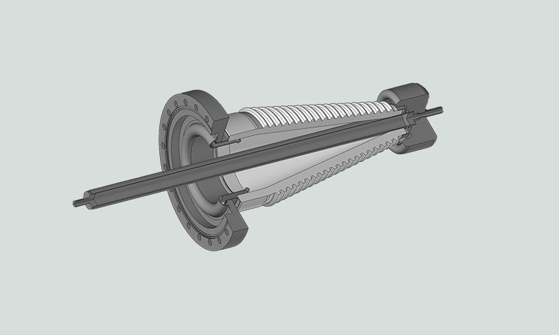
For decades Kyocera has produced high-voltage (30kV or higher) ceramic feedthroughs to meet customer requirements.
We have developed design and simulation technology, ceramic materials for higher voltages, and a performance evaluation system that covers a wide variety of product shapes and specifications. We solve various problems of high voltages for our customers.
Kyocera's 3 Solutions
Consulting with our team - from the initial design stage of high-voltage products to reducing the risk of discharge breakdown.
< Needs for High Voltage Components >
- Stable maintenance of high voltage
- Reduction of conditioning time
- Compact and space-saving designs
- Leak current reduction
- Longer life
< Kyocera's Support >
- Design technology of high-voltage ceramic components
- Optimum material proposal for the application
- Performance evaluation of high voltage products
1.Design Technology of High-Voltage Ceramic Components
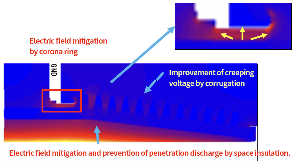
It is possible to carry out electric field simulation based on product shape. We can propose a robust high voltage insulator design structure based on our abundant experiences.
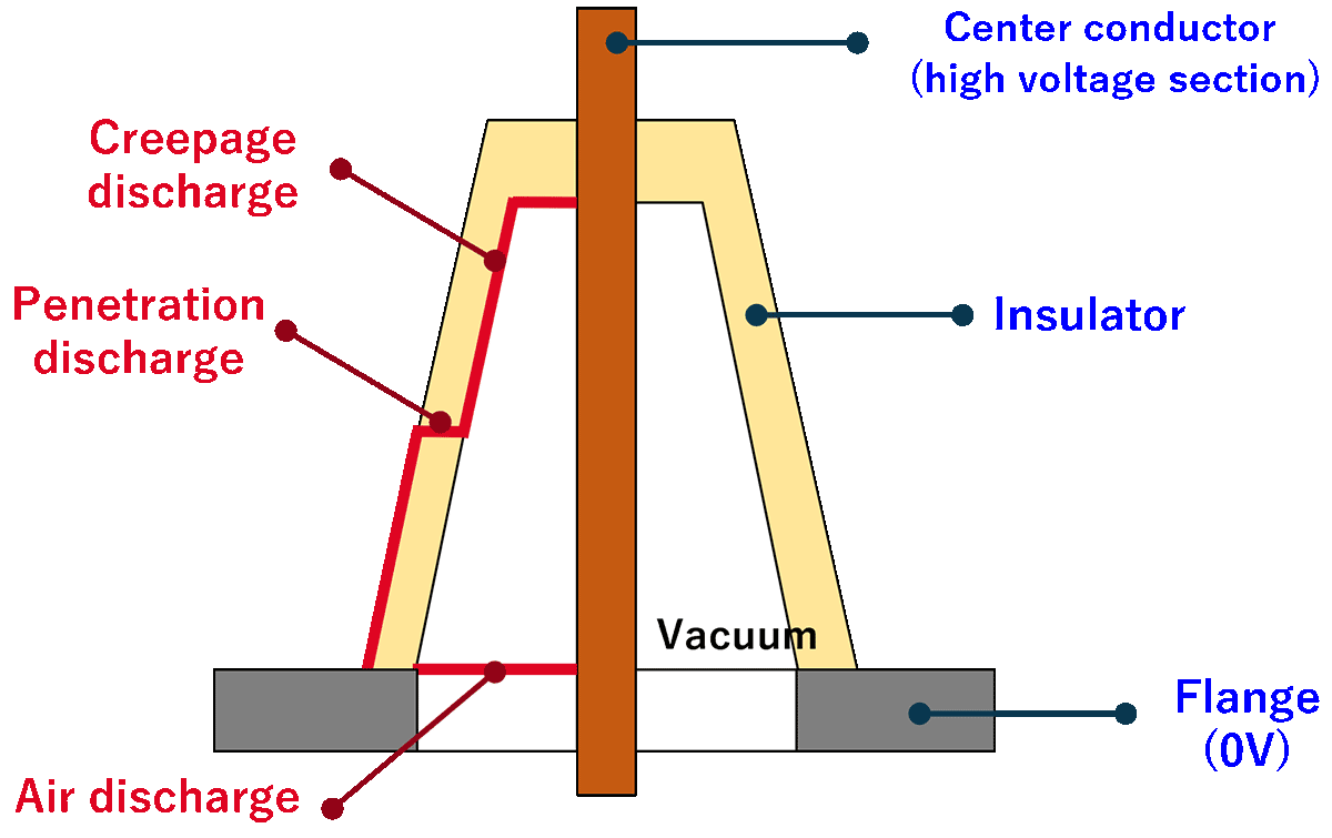
Understanding product weaknesses by electric field simulation
Type of high voltage insulator discharge
Voltage resistant design structure incorporating ceramic technology
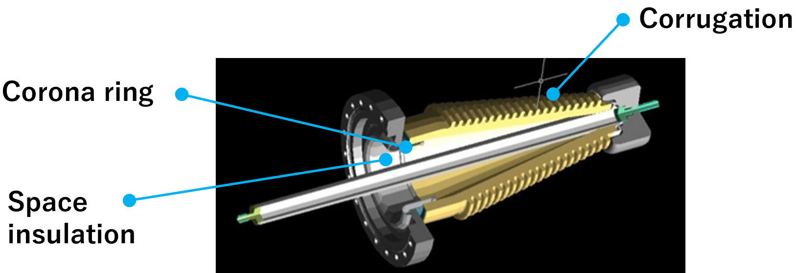
- Corrugation for creeping voltage insulation
- Electric field relaxation by corona ring
- Selection of alumina (by dielectric constant and resistivity)
- Optimization of metallization range (field mitigation)
Example of 100 kV feedthrough
Proposal of design structure for voltage resistance
- Corrugation
- Corona ring
- Space insulation
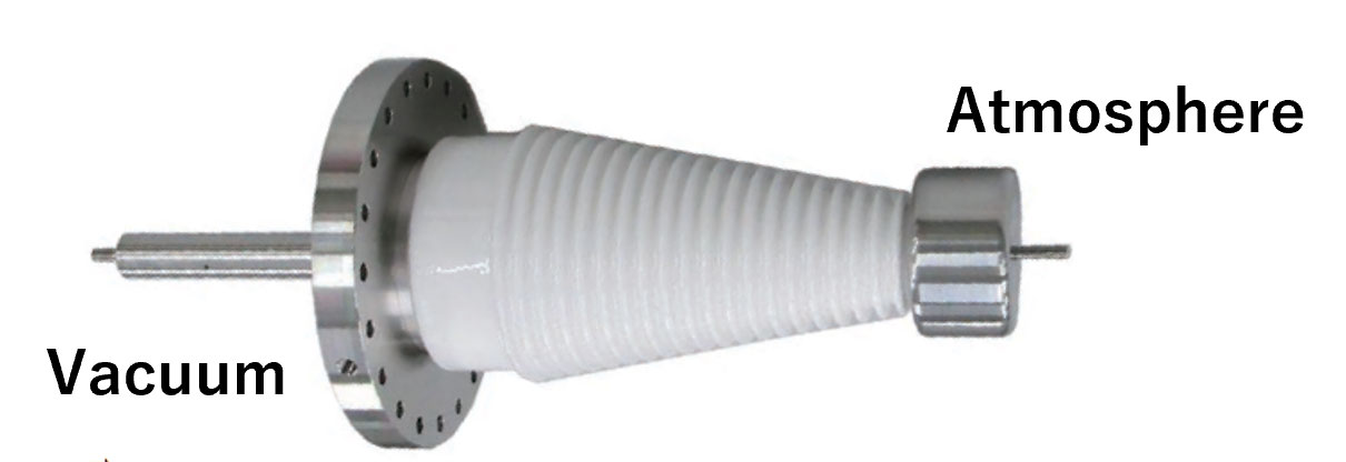
Design proposal for high voltage standoff
Electric field simulation
2.Optimum Material Proposal for Each Application
We propose the most suitable ceramic, from a wide range of materials, according to the required characteristics.
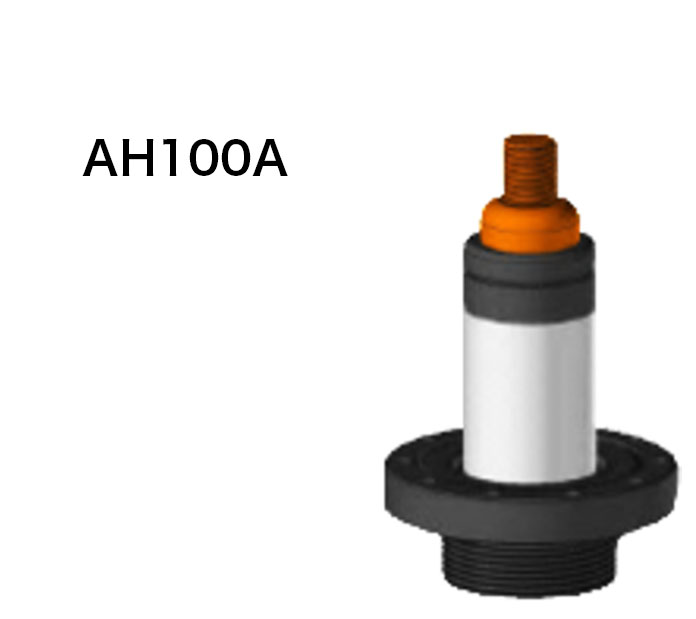
In this section, we will introduce the expected effects of replacing the conventional alumina material with the “high voltage-resistant alumina AH100A” material (reduction of component size and conditioning time).
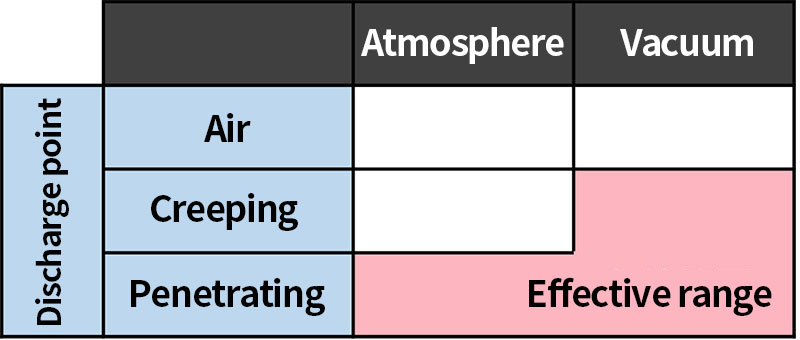
Improvement of voltage resistance performance
Creeping dielectric resistance (in vacuum)
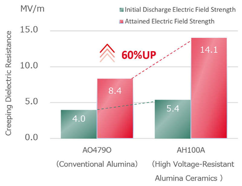
Creeping dielectric resistance distance: 2 mm
Degree of vacuum: 10-4 Pa or less
Other measurement conditions of Kyocera
Penetrating dielectric resistance
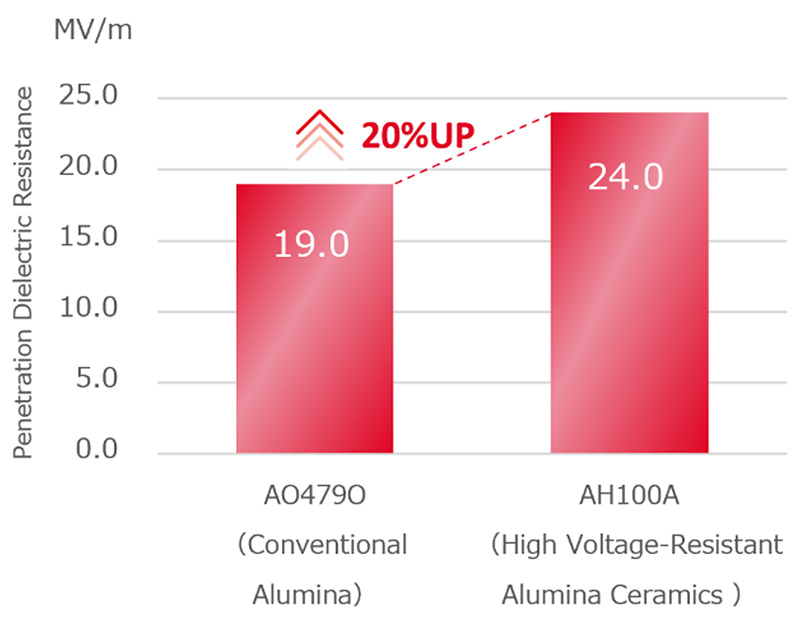
Sample thickness: 1 mm
Other JIS C 2141 compliance
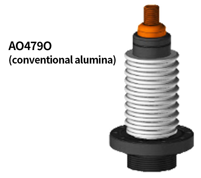
Miniaturization
50% reduction in ceramic parts due to improved voltage resistance*Kyocera's calculation
Image
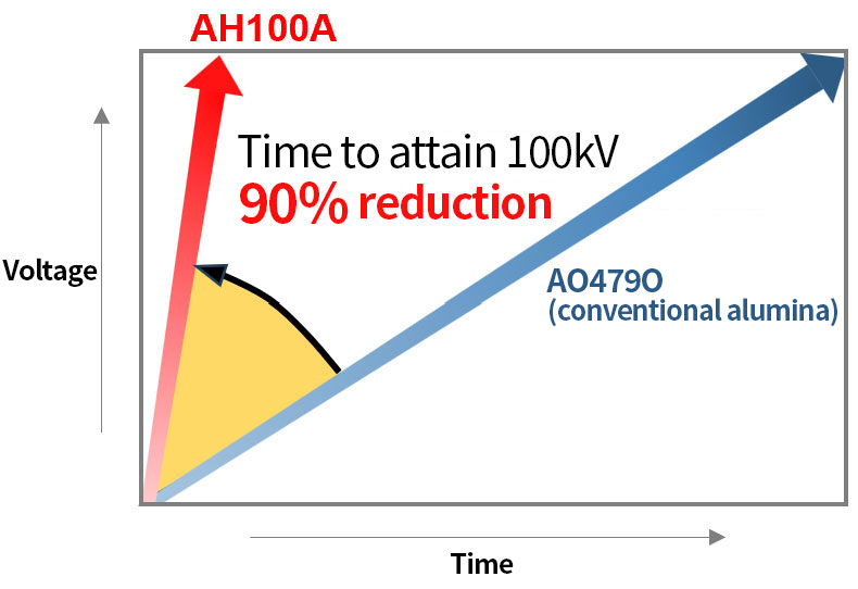
Reduction of conditioning time
Significant reduction in conditioning time to high voltage (approximately 1/10th the time compared with conventional alumina A479)
High voltage insulator spark conditioning time
Elevated voltage speed: 1kV/min
Hermeticity: 10-3 Pa or less
Conditions that are effective for voltage resistance performance
Metallization type of AH100A: Ag-Cu-Ti
3.Performance Evaluation of High Voltage Products
We have equipment to measure high voltage resistance and hermeticity. Performance evaluation can be conducted by making customized fixtures.
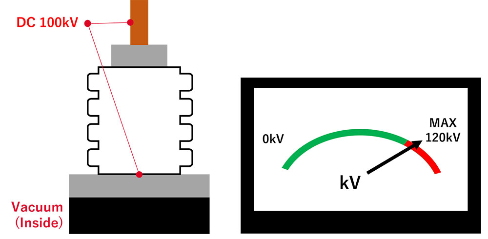
High-voltage DC test
Kyocera is able to test up to MAX DC120kV. For higher voltage design, please contact us.
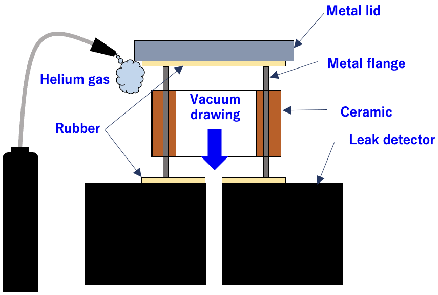
Helium leak test (Hermeticity: < < 1.0 x 10⁻¹⁰ Pa · m3/s)
All values listed on this page are representative values obtained from in-house measurements,
and do not constitute guaranteed product specifications.
