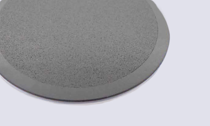
Kyocera's new semiconductive ceramic coating provides static elimination by depositing a semiconductive ceramic coated film on the surface of the base material. If the film thickness is 50 μm or less, it has air permeability, so it is used for wafer vacuum chucking parts with porous ceramics to prevent electrostatic breakdown.
Features
- Semiconductivity function can be added
Electric resistance of the coated film can be kept within a range of 105 to 1010 [Ω]. - Stable electric resistance
Small dispersion of electric resistance within the same surface. - Highly precise surface processing is possible
The high rigidity and hardness of the ceramic-coated film allow for the lapping process after coating.
Stable Electric Resistance
Low variation within the coated surface and stable electric resistance can be achieved.
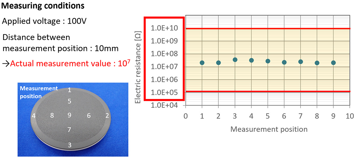
*Results may vary depending on product specifications and usage conditions.
Coating Condition
Size: Please consult (we have experience up to 12 inches in diameter)
Thickness: 500 μm or less
*Depends on the type of ceramic material.
*If the thickness is less than 50 μm, air permeability can be ensured when applied to porous materials.
If the shape is complicated, it may be difficult to apply.
Coating Process
Coating process image of wafer chuck
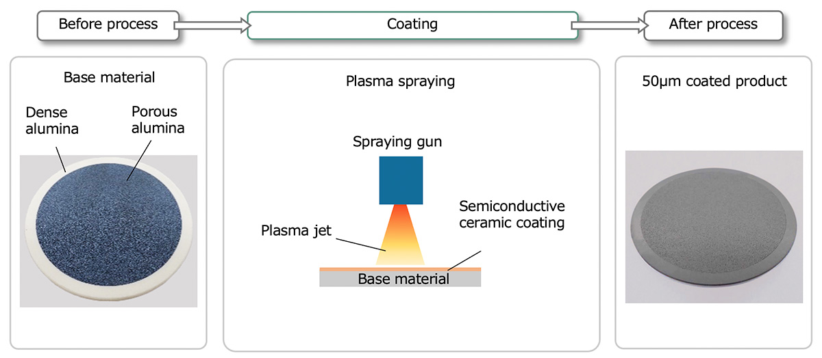
Process Example
We have experience applying this technology to wafer transfer pads, wafer chucks for processing, and other components that require static elimination functions.
It can be applied to handling arms.
-
Wafer transfer pad
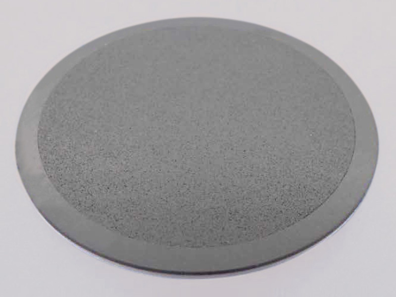
Size: φ128 x t10 (mm) Base material: Alumina(A479)
+Porous alumina(#100)Film thickness: 50μm -
Wafer chuck for processing
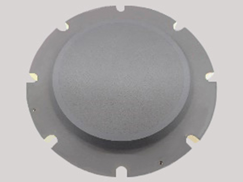
Size: Φ235 × t30 (mm) Base material: Alumina(A479)
+Porous alumina(#100)Film thickness: 50μm
All values listed on this page are representative values obtained from in-house measurements,
and do not constitute guaranteed product specifications.
