
Simulation to Optimize Design
Kyocera offers various electrical, thermal, and mechanical simulations to ensure the design we propose will meet your specific requirements.
Electrical Simulations
Click Here for High-Frequency Device Design Support
Thermal Simulation
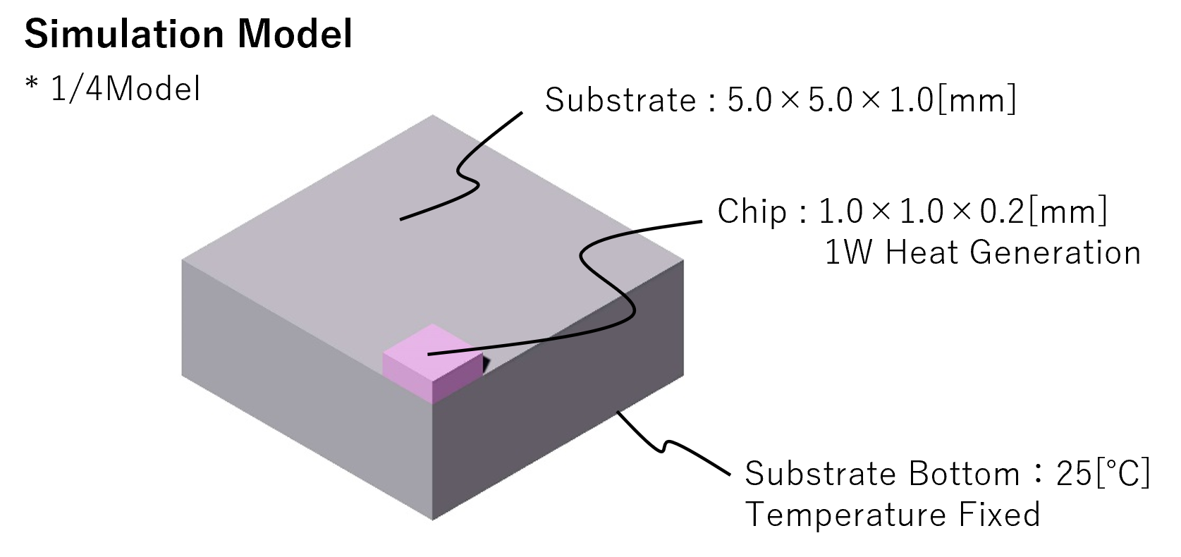
Difference in Temperature Change by Material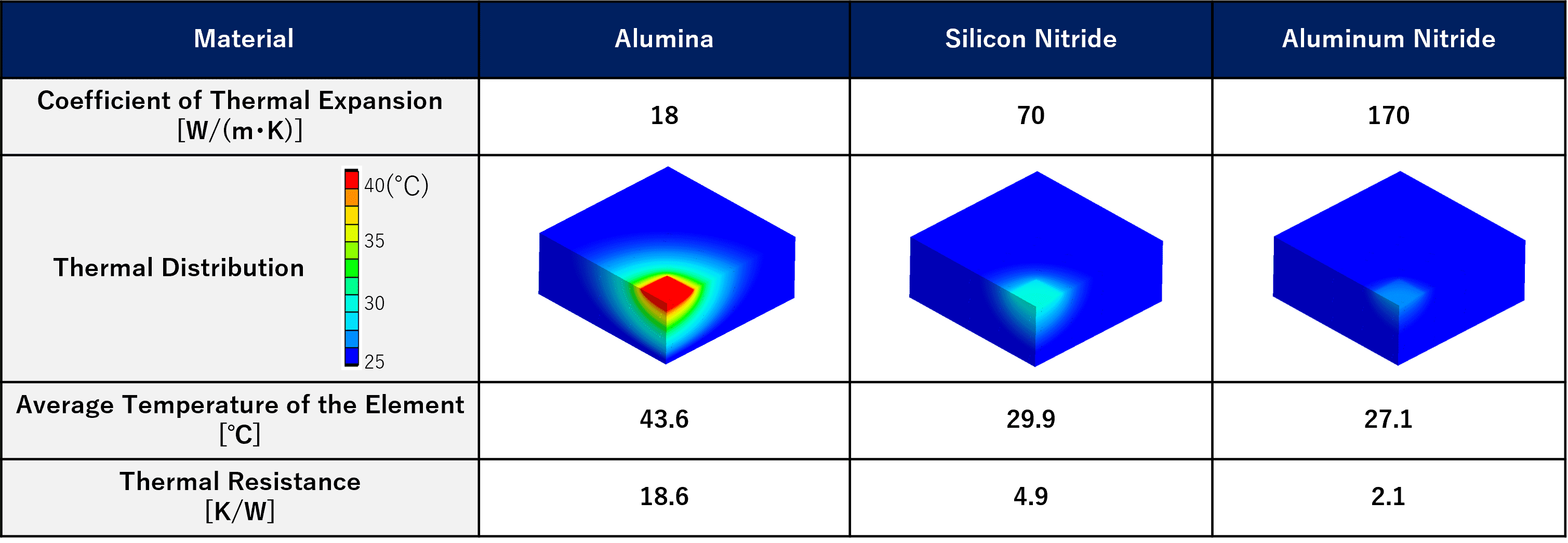
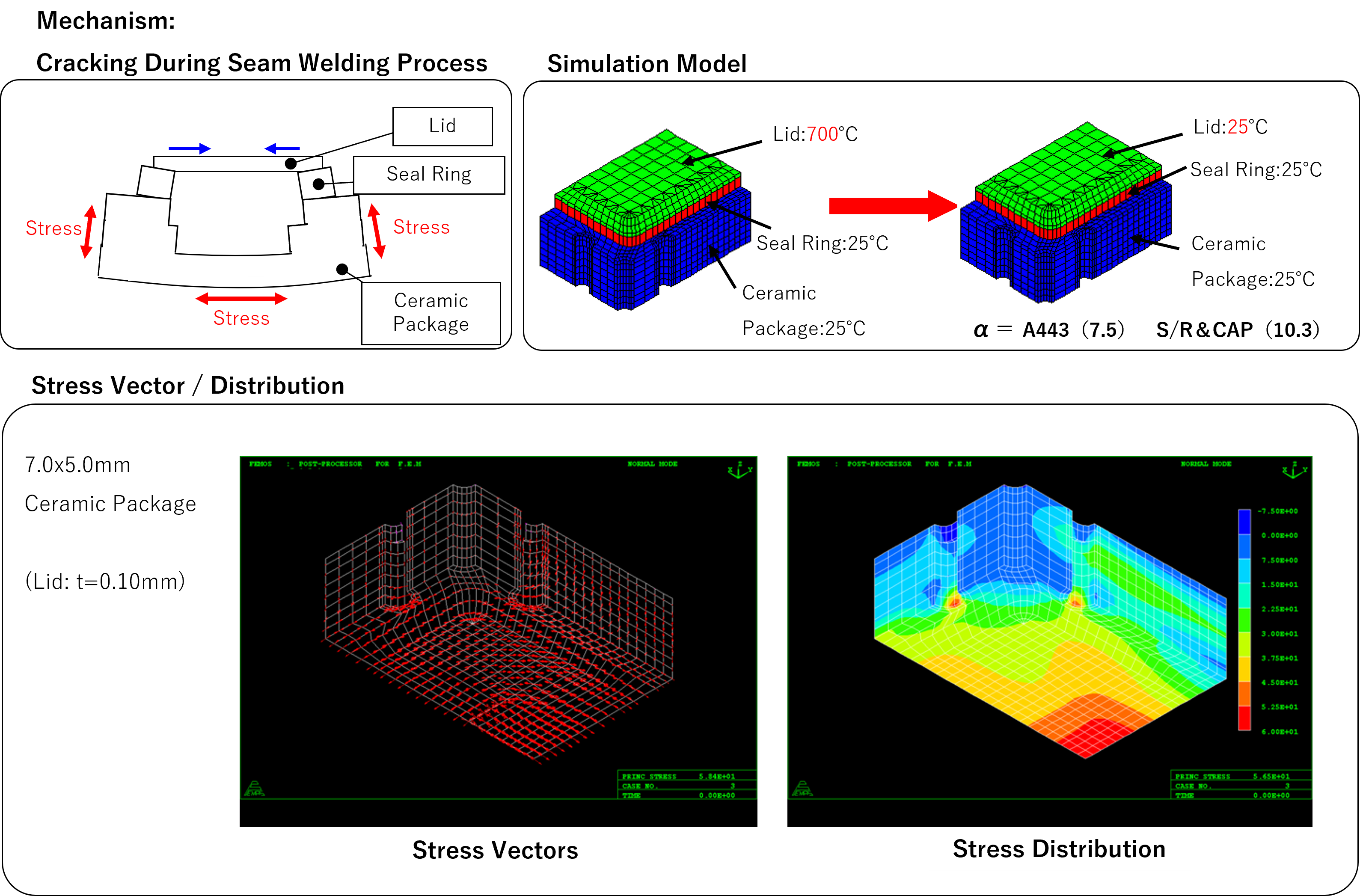
Stress Simulation
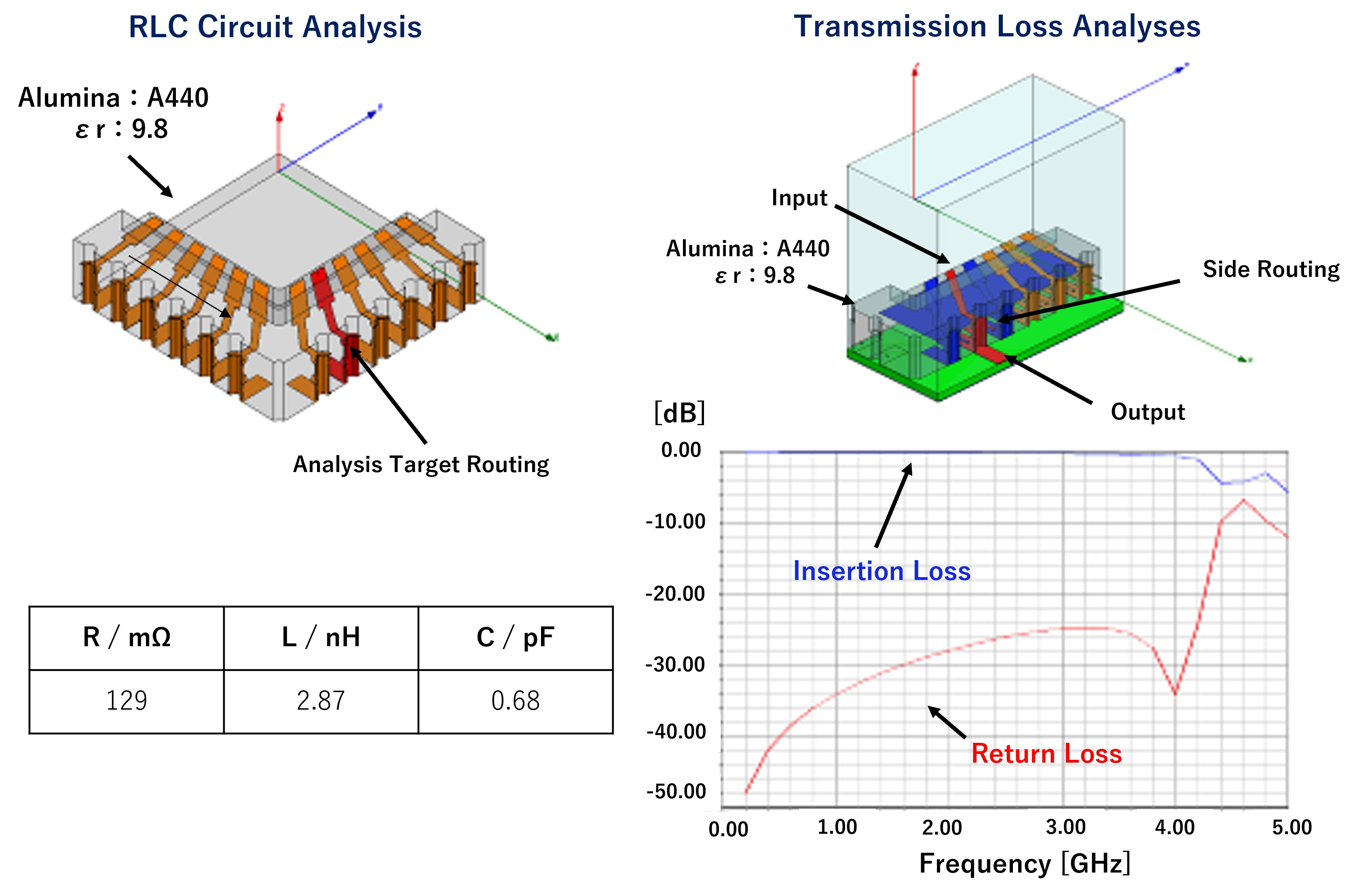
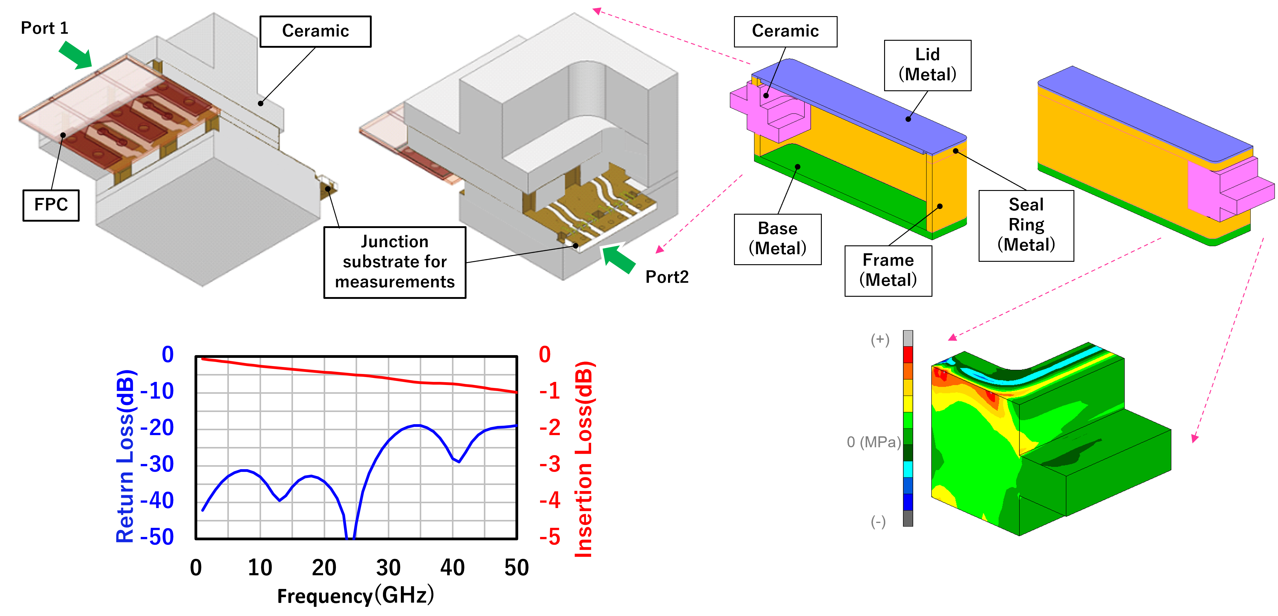
Examples: Electrical Simulation / Thermal Simulation
The example below shows an analysis of Kyocera's package for a QSFP28 optical transceiver. Kyocera designed its high-frequency characteristics using electromagnetic field simulation of a model including a junction substrate (left). We also conducted thermal stress simulation (right) to confirm that the product has both high-frequency characteristics and a structure with low residual stress.
Contact us for details on various simulations.
Other Key Technologies Supporting Innovation
Thin-Film Technology
Ceramic Package Features and Basic Structure
Wiring Technology: (Thick / Thin Film)
Material Options
Bonding Dissimilar Materials
Offering a Wide Variety of Package Designs and Structures
Co-Firing Technology
Plating Technologies for Multilayer Ceramic Packages
3D Structures / 3D Electrical Interconnects
Customized Optical Window Lid Design