
Ceramic Package/Substrate Wiring Technologies
Thick-Film Printing
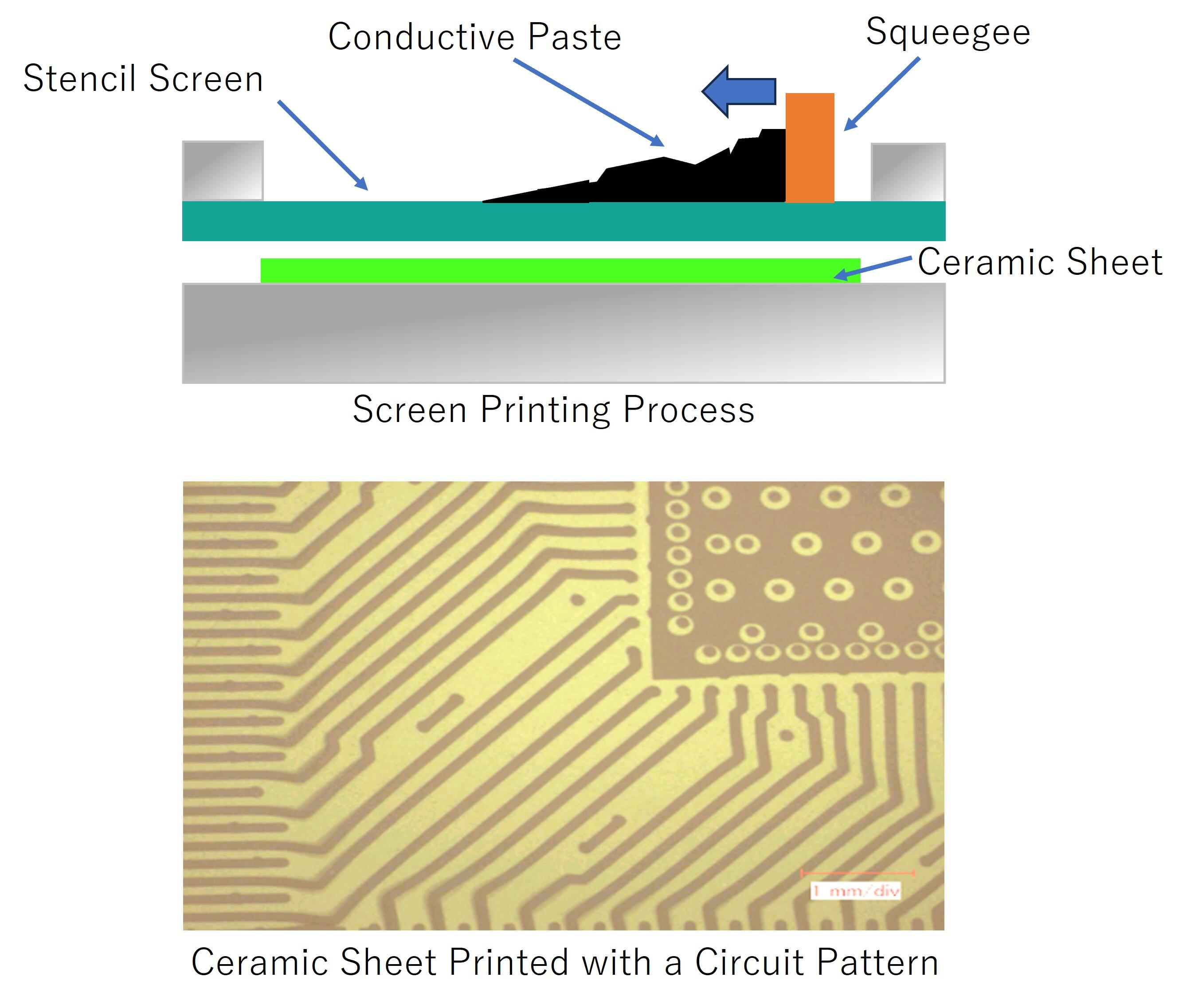
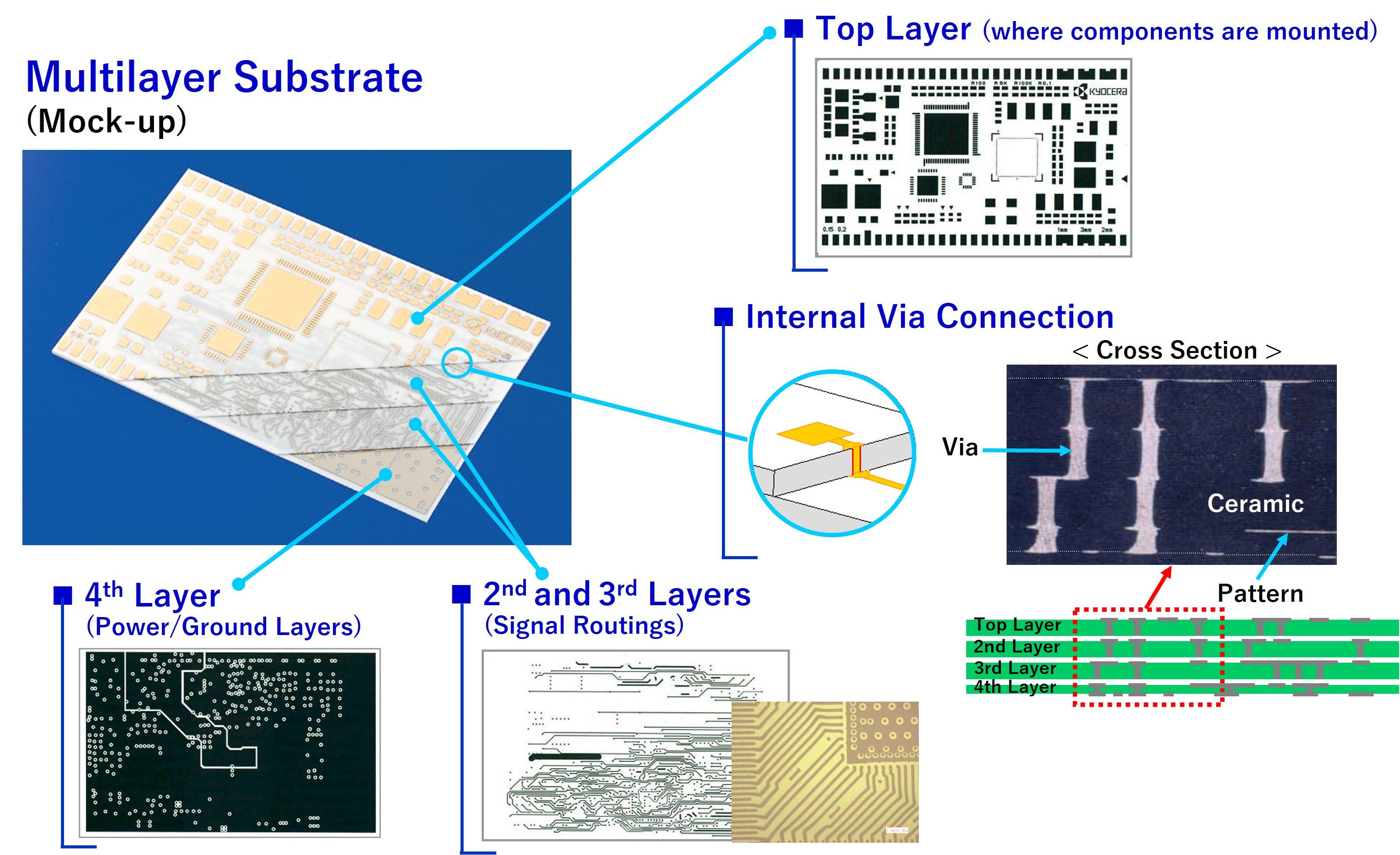
In the ceramic multilayer manufacturing process, conductive paste is screen-printed onto each layer to form an electrical circuit pattern. Vias in the ceramic sheet are filled with conductive paste, achieving electrical connections between layers. By co-firing after laminating these layers, a three-dimensional electrical circuit is created within a ceramic multilayer package.
For details about this manufacturing process, click here.
Note: Screen printing creates wiring patterns by applying conductive paste onto the sheet through the openings in a stencil screen.
Examples of 3D Electrical Interconnects in Ceramic Multilayer Substrates
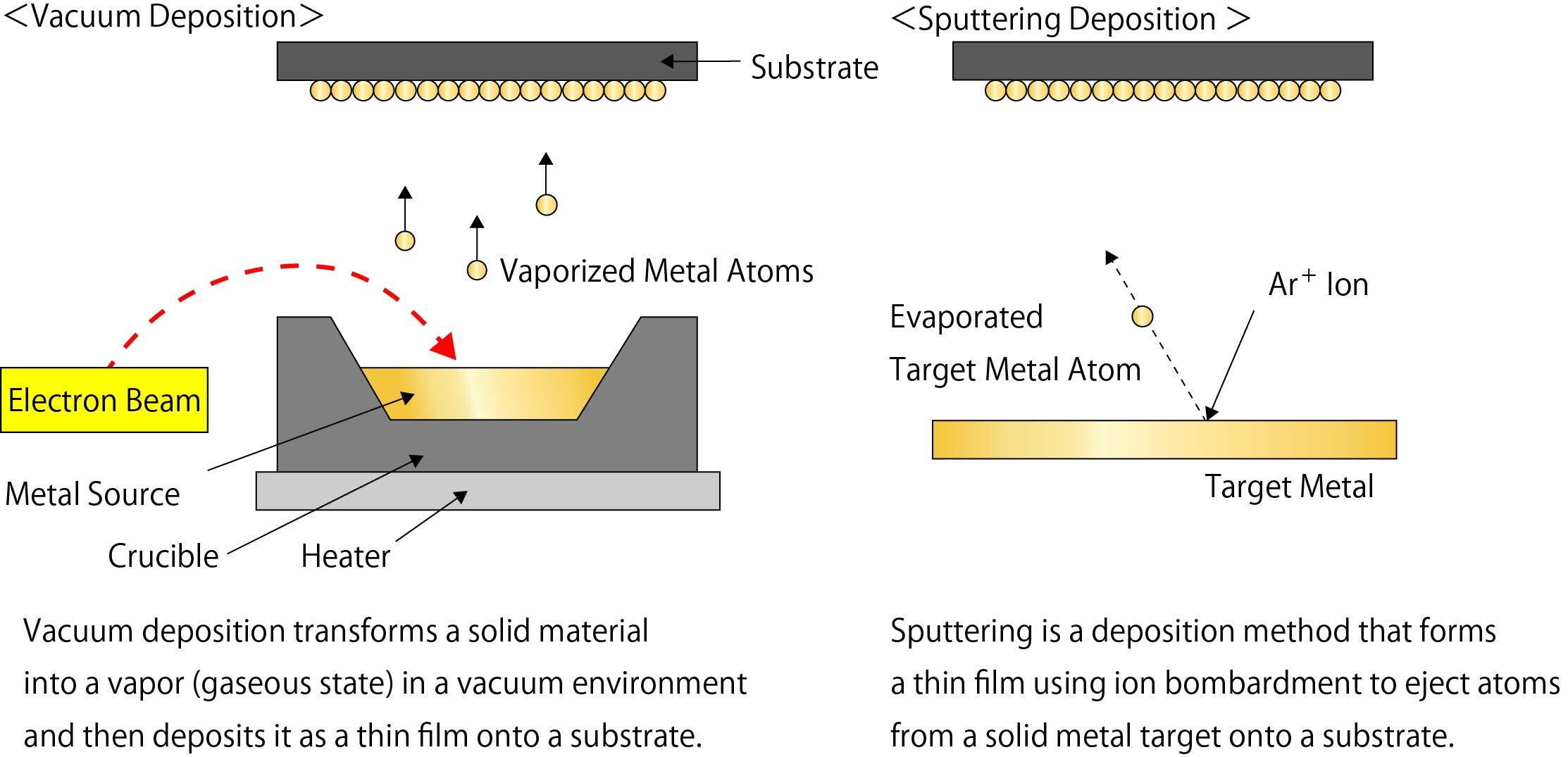
Thin-Film Processing
By utilizing thin-film processing, fine circuit patterns with very high positional accuracy can be formed on a polished ceramic substrate surface. Kyocera offers thin-film processing on ceramic substrates through vacuum deposition or sputtering methodologies. Various ceramic materials, film configurations, and processing technologies can be combined in optimal ways to meet your custom requirements.
For details on thin-film technology, click here.
For details on thin-film substrate manufacturing technology, click here.