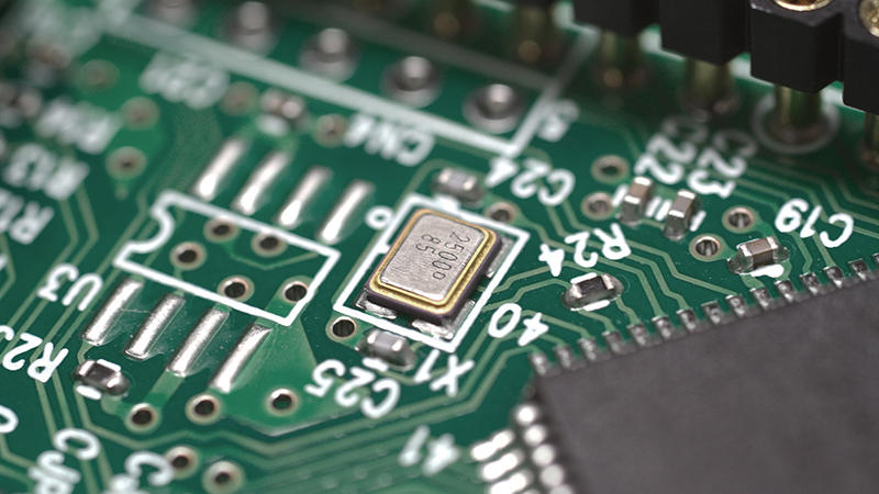
Manufacturing Process: Thin-Film Ceramic Substrates
This is an example of the manufacturing process for thin-film ceramic substrates.
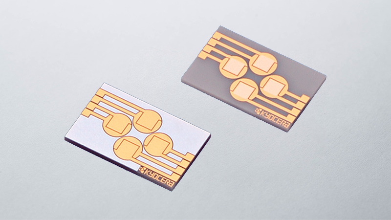
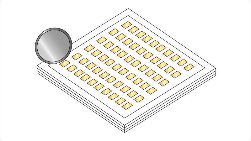
*Thin film can be metallized onto both single-layer and multilayer ceramic substrates.
Learn more about thin-film metallization technologies here.
*Thin film can be metallized onto both single-layer and multilayer ceramic substrates.
Learn more about thin-film metallization technologies here.
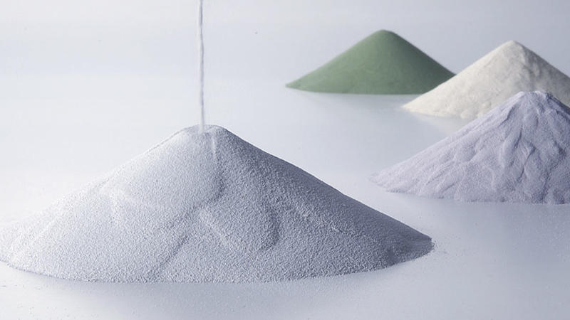
1. Powders / Formulations
Raw materials are mixed.
2. Tape Casting
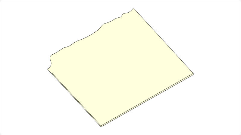
Mixed materials are formed into a tape.
3. Via Punching / Filling
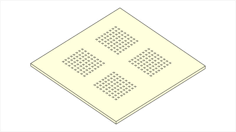
Tape is punched with tooling to create circuit via holes, which are filled with conductive paste to provide electrical connections through the tape.
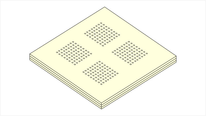
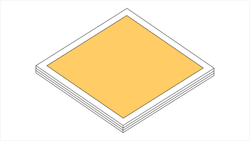
4. Pattern Printing
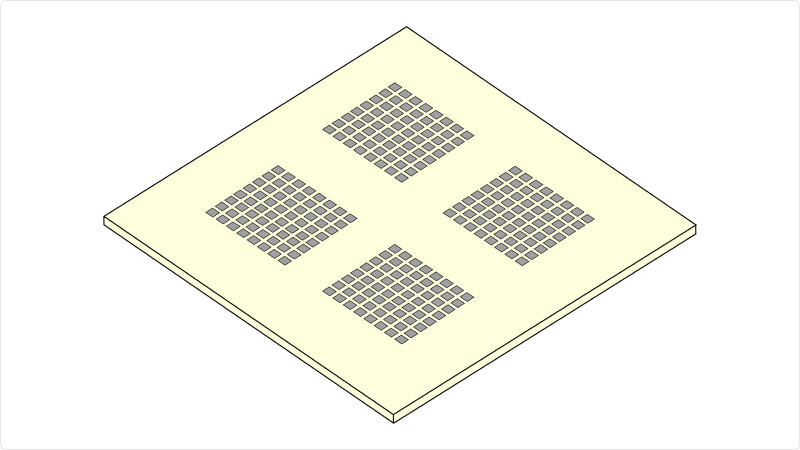
Circuit patterns are printed on the surface of each layer.
5. Lamination
Processed tape is stacked into layers and laminated to form 3D circuits within the structured ceramic board.
6. Cutting
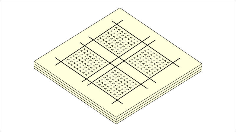
Laminated sheet is cut into individual substrates for co-firing.
7. Co-Firing
Individual substrates are co-fired in a furnace at high temperature.
8. Grinding
Grinding surface ensures the flatness of the substrate for thin-film application.
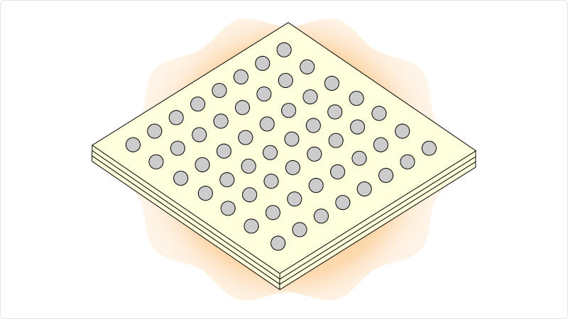
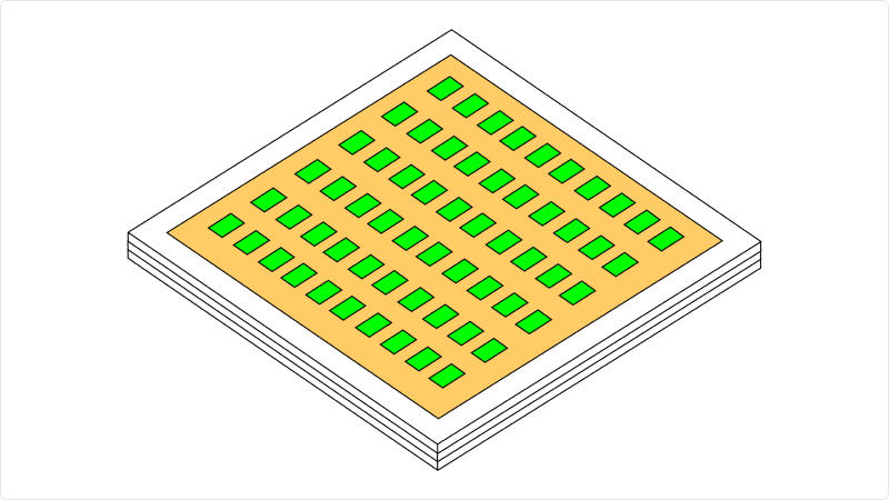
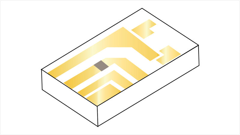
9. Thin-Film Deposition
(Evaporation/Sputtering)
(Evaporation/Sputtering)
Film is deposited by evaporation or sputtering.
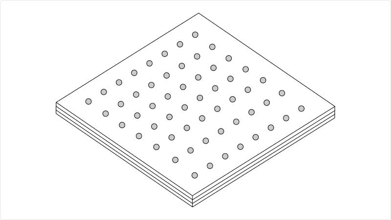
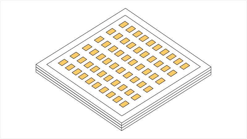
10. Photolithography
Photoresist is applied to the substrate and exposed.
11. Etching
Metals on areas without photoresist are removed with a chemical etching process, and photoresist is removed.
12. Plating
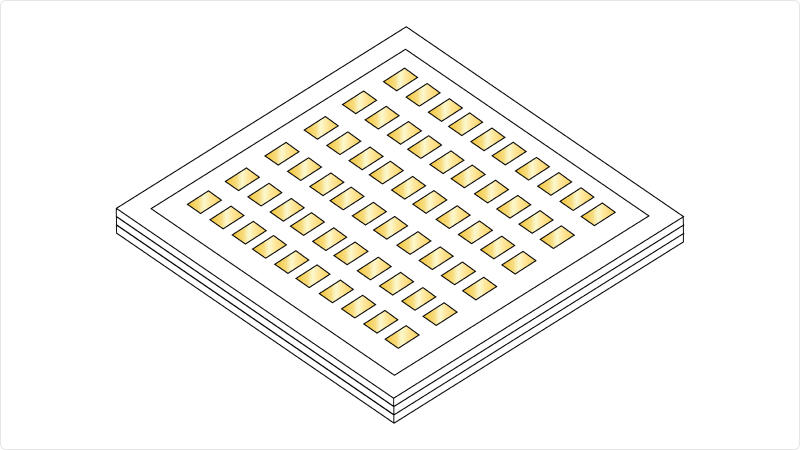
Plating metal combinations are determined by customers' functional requirements.
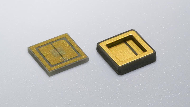
13. Dicing
Substrate is simulated into individual units.
14. Inspection/Packing/Shipping
Finished substrates undergo final inspection, then are packed into boxes and shipped.
*Processes after thin-film deposition are typical examples for standard products.
Process details differ depending on thin-film composition and substrate design customization.
Process details differ depending on thin-film composition and substrate design customization.