Manufacturing Process: Ceramic Multilayer Packages
Below is an overview of Kyocera's manufacturing process for ceramic multilayer packages.
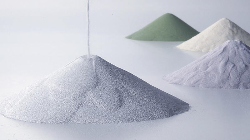
1. Powder Mixing
Raw material powders are blended.
2. Tape Casting
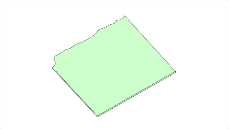
Mixed raw materials are formed into a tape and cut into sheets.
3. Punching
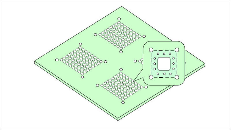
Sheets are punched with tooling to create vias and holes for device cavities and via routing.
4. Via Filling
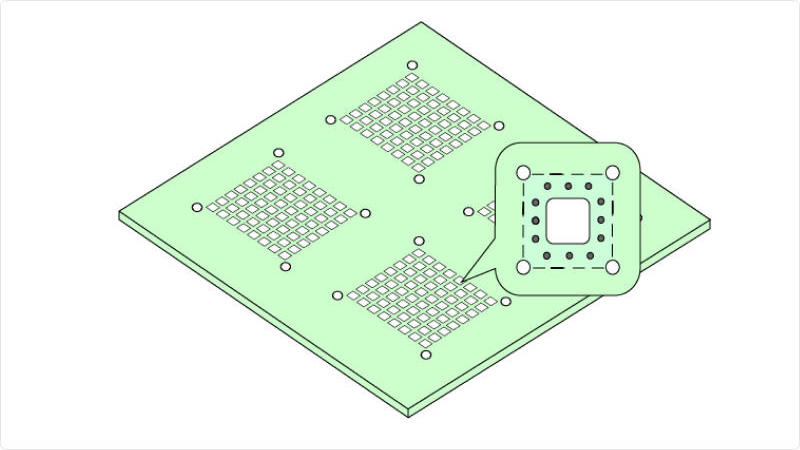
For electrical conductivity between layers (in the vertical direction), vias are filled with conductive paste.
5. Screen Printing
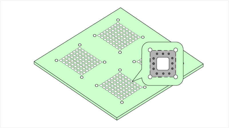
Conductive paste is printed into a circuit pattern on the sheet surface (in the "X" and "Y" directions).
6. Lamination
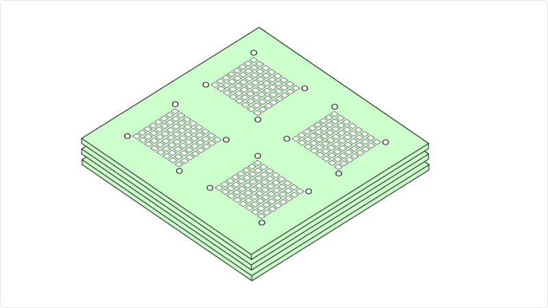
Processed sheets are stacked into layers and laminated.
7. Snap
Grooves are made to allow substrate arrays to be separated after the co-firing process.
8. Cutting
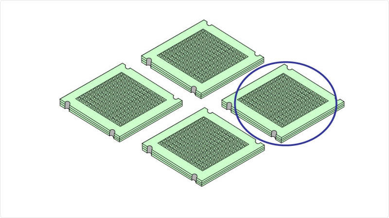
Substrate arrays are separated for adequate size for co-firing.
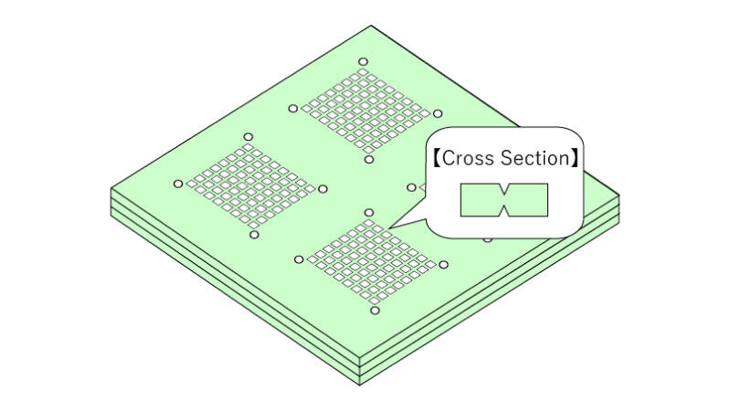
9. Co-Firing
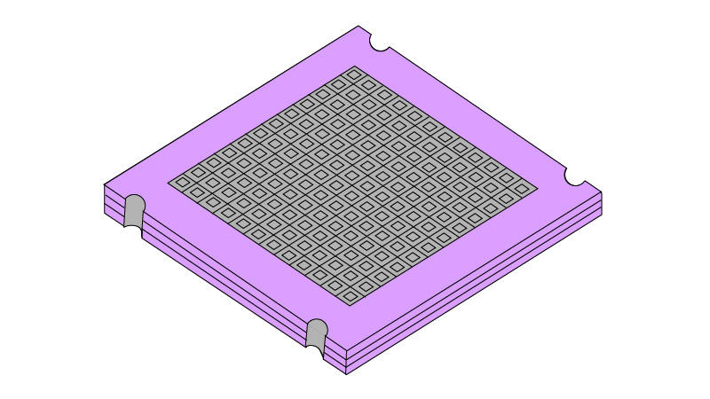
Substrate arrays are co-fired in high-temperature furnaces.
10. Ni Plating
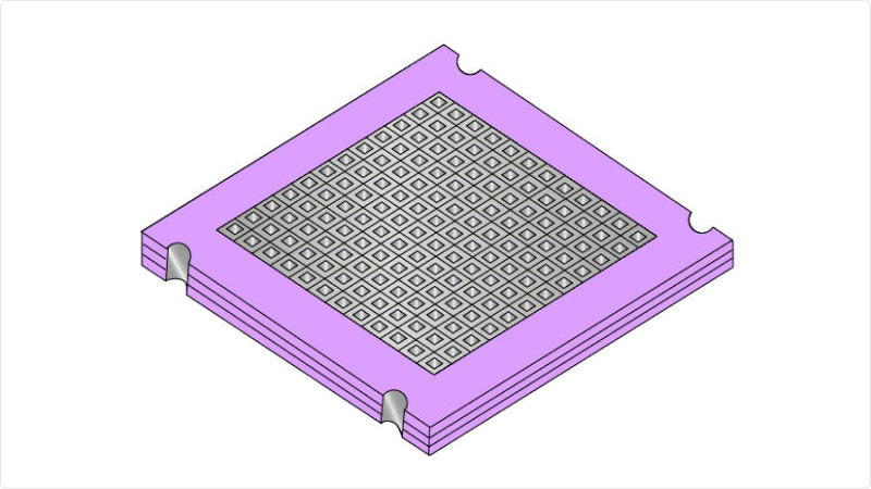
Metallization area on substrate arrays are plated with nickel.
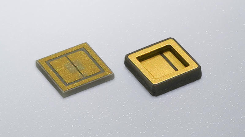
11. Metal Assembly
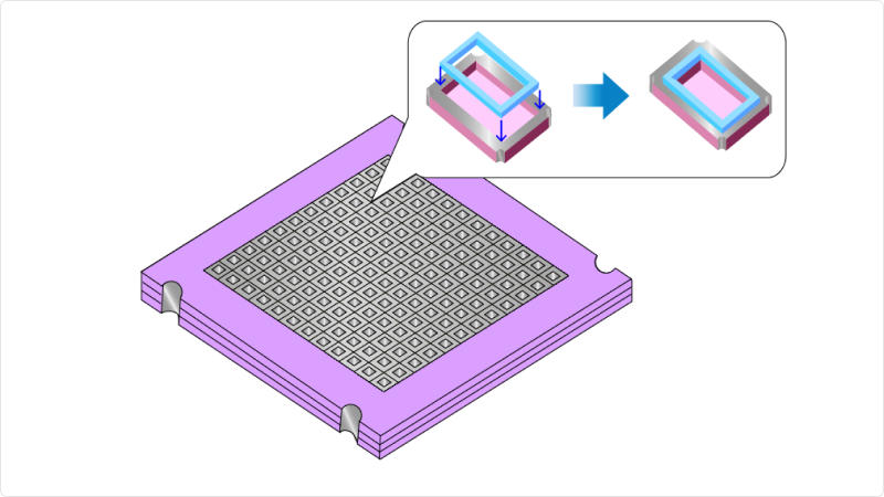
Metal parts are brazed to the nickel plated substrate arrays.
12. Final Ni and Au Plating
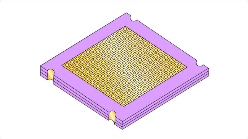
Nickel and gold are plated after the brazing process.
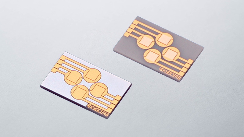
13. Singulation
Individual substrates are separated by breaking along snap grooves.
14. Inspection/Packing/Shipping
Once singulated, ceramic multilayer packages are inspected, packed, and shipped to the customer.