What Are Semiconductor Packages? / What is Packaging?
A semiconductor package is the "case" that protects IC chips and other components while connecting them to a circuit board. Semiconductor packages are made from such materials as metal, plastic, glass, and ceramics.
The Roles of a Semiconductor Package
- Protects IC chip(s) from environmental influence, including moisture, dust, light, and electromagnetic interference.
- Protects IC chip mechanically.
- Provides input/output signals and required isolation.
- Dissipates heat generated by IC chips.
About Packaging
What is Chip-Level Assembly?
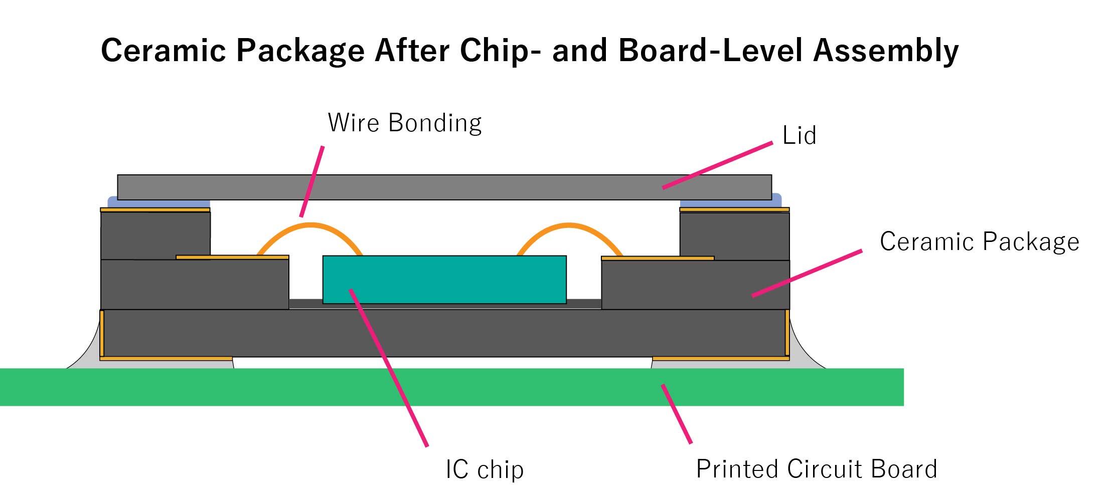
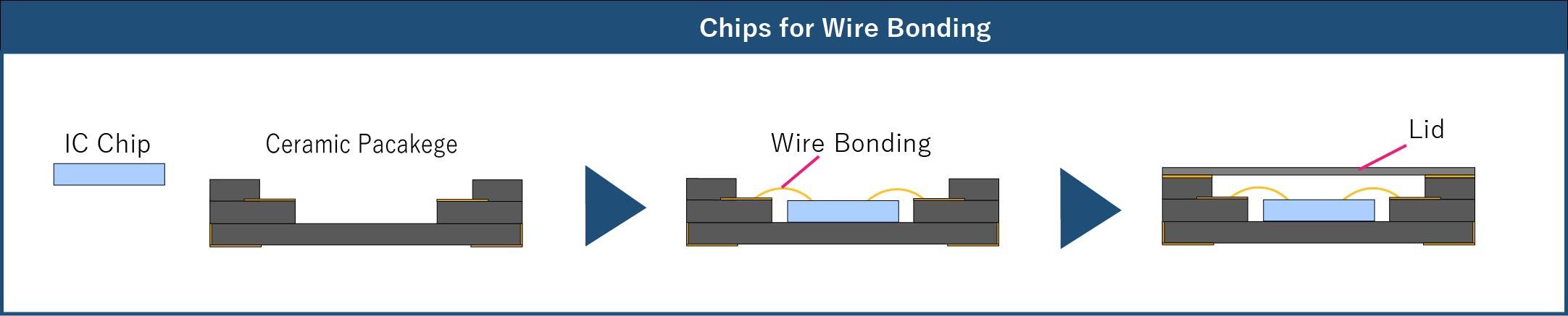
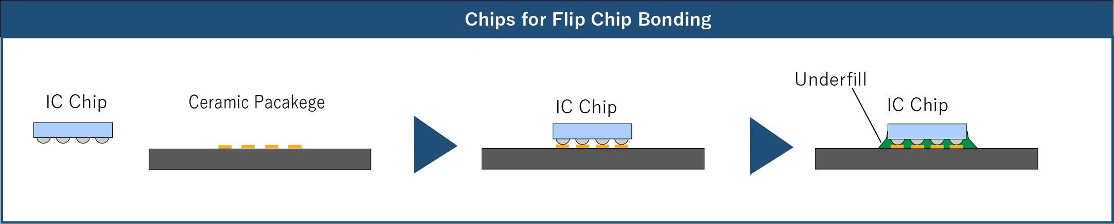
Chip-level assembly involves mounting the IC chip(s) onto the package.
Chip-Level Assembly
What is Board-Level Assembly?
Board-level assembly involves mounting the packaged device(s) onto the printed circuit board. This process physically affixes and electrically connects the package to the board.
Board-Level Assembly (Surface Mount)

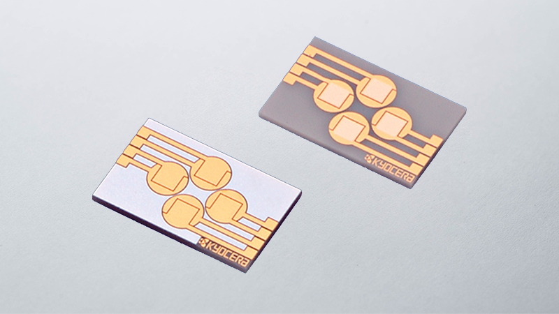
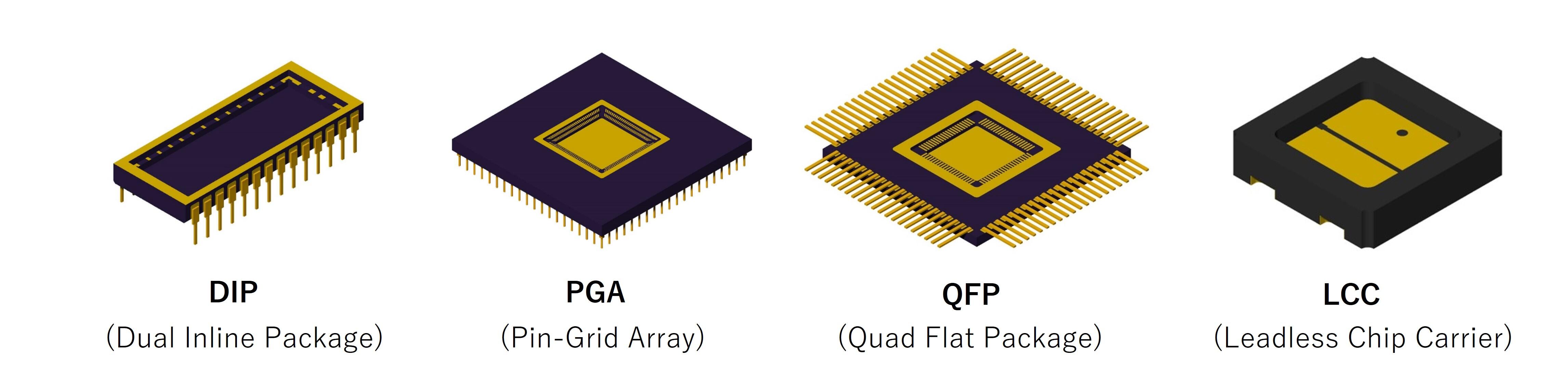
Ceramic Package Configurations
Ceramic packages are available in many configurations to support various board-level assembly options, including Dual Inline Packages (DIPs); pin-insertion configurations, such as Pin-Grid Arrays (PGAs); Quad Flat Packages with leads (QFPs), surface-mount Quad Flat Non-Leaded Packages (QFNs); Ball-Grid Arrays (BGAs), Chip Scale Packages (CSPs), and Leadless Chip Carriers (LCCs).
What Are Ceramic Packages?
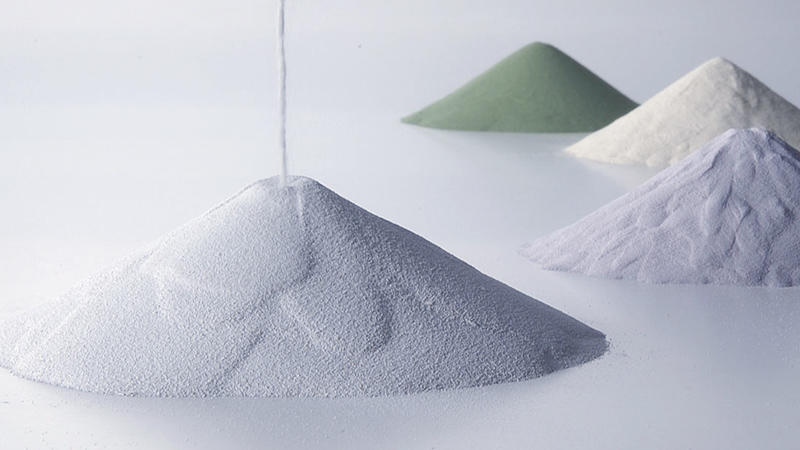
Semiconductor packages can be made of organic materials (including plastics), inorganic materials (including ceramics), and/or metals, depending on the device’s application and performance requirements. Ceramic packages are made of Fine Ceramics*.
Kyocera’s ceramic packages are used in many fields due to their higher strength, higher thermal conductivity, design flexibility, and thermal characteristics, including coefficients of thermal expansion (CTE) closely matching those of the most common semiconductor materials. Their applications range from mass-produced products to precision equipment requiring the highest reliability. Click here for more application examples.
*Ceramics refer to “non-metal, inorganic materials manufactured through a high-temperature firing or sintering process.” This definition may apply to ceramics, glass, cement, bricks, enamels, and graphite; those with the most advanced material properties and highest dimensional precision are called Fine Ceramics.
Features of Kyocera’s Ceramic Packages
-
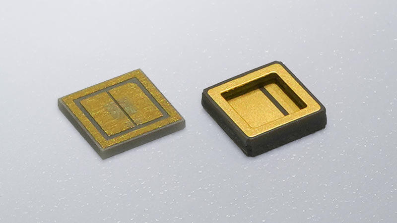
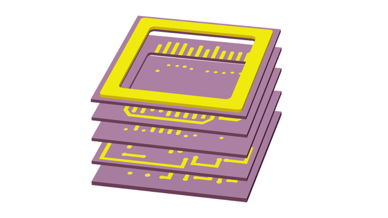
Flexible Design OptionsBecause Kyocera’s process involves laminating many layers of ceramic, it allows three-dimensional packages to be created with three-dimensional electrical routing. It also facilitates miniaturization, lower inductance, cavity structures (hollow box shapes), and designs tailored to any chip, with limitless freedom in terminal arrangement.*Click here for the ceramic package manufacturing process.
-
Broad Material OptionsKyocera offers a wide variety of ceramic materials to achieve your performance requirements, with superior thermal conductivity, coefficients of thermal expansion, and high-frequency characteristics.* Click here for a material properties table.
-
Electrical PropertiesThree-dimensional electrical routing and structures make it possible to design for specific electrical properties. We also have low-tanδ LTCC materials.* Click here for details of LTCC materials.
-
Thermal PropertiesHigh thermal conductivity: We can offer materials with excellent heat dissipation.*Click here for details.Coefficient of Thermal Expansion: We can offer materials with coefficients of thermal expansion closely matching either the semiconductor chip or the PCB. Ceramics do not warp easily, even when heated, thus stabilizing device properties.*Click here for details.
-
Mechanical CharacteristicsAs semiconductor package materials, ceramics offer superior properties of strength, stability, rigidity, and Young’s Modulus. Their high strength allows thinner cavity walls, enabling new levels of device miniaturization.
-
Chip- and Board-Level Assembly OptionsCeramic packaging supports many chip- and board-level assembly options.・Chip-level assembly options include wire bonding and flip-chip bonding.・Board-level assembly options include LCC, QFP, PGA, DIP, BGA, and others.*Click here for Kyocera’s standard products.
-
Enabling Smaller, Thinner PackagesMultilayer ceramics facilitate miniaturization. Electrical circuit patterns are applied to each layer and then laminated, resulting in space-saving and three-dimensional routing. Ceramics feature high rigidity as well, with warp resistance even at very thin dimensions. Additionally, ceramics allow inter-layer connections (vias) to be formed with great freedom of design and precision on each layer as a standard feature.* Click here for high strength materials.