Customized Solutions: Ceramic Packages Integrated with Thin Films, and Other Process Technologies
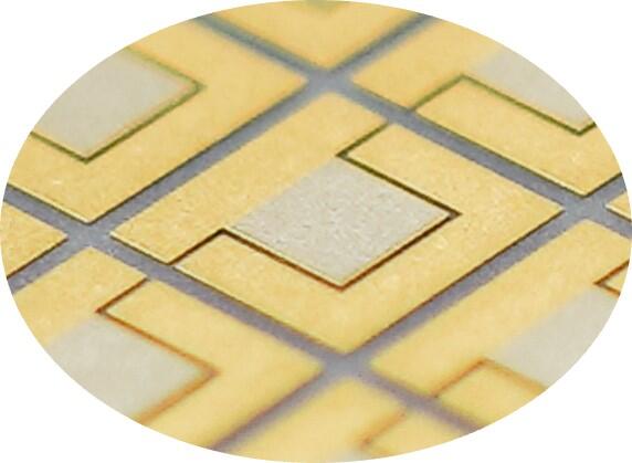
Applying thin-film processing to ceramics can provide much finer, higher-precision patterns than those attainable from screen-printed thick-film technology in multilayer ceramic structures. Kyocera can customize a microelectronic packaging solution to your requirements using a combination of multilayer ceramics, thin-films, and advanced processing technologies.
Ceramic Materials Suitable for Thin-Film Processing
- Alumina (Al2O3)
- Aluminum Nitride (AlN)
- Silicon Nitride (Si3N4)
Thin-Film Composition Options
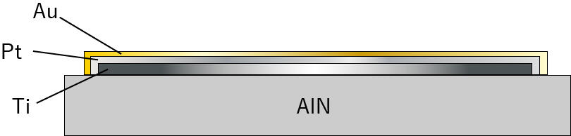
Example of Film Deposition
- Ti-Pt-Au
- Ti-Pd-Au
- Ti-Al
- Ti-TiW-Cu-Ni-Au
- Ti-TiW-Cu-Ni-Pd-Au
*Not all thin-film combinations are suitable for use on all ceramic materials. Please contact us for details.
Processing Technology
We can propose solutions for integrated processing technologies to meet your specific requirements.
Thin-Film Resistors/Trimming
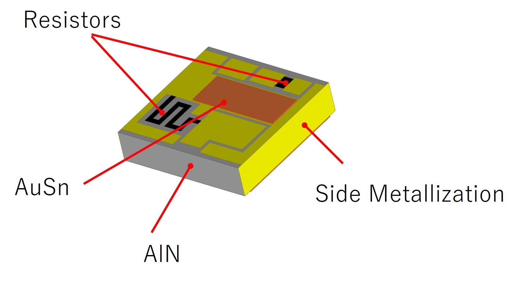
For high-frequency circuits, thin-film resistors can be deposited directly onto a substrate for impedance matching.
Au-Sn Deposition
Depositing Au-Sn directly onto a substrate can allow mounting without AuSn preforming during assembly.
Conductive Vias
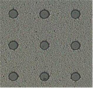
Tiny vias can be formed in a substrate and filled with conductive paste to create high-precision electrical connections between substrate top and bottom surfaces.
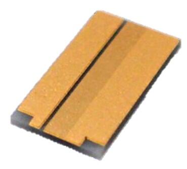
Steps and Grooves
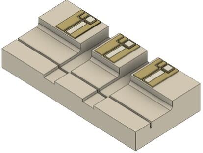
Steps and grooves with high dimensional accuracy can be added to a ceramic substrate. Example: Steps and grooves for lens mounting on RGB laser substrates.
Side Metallization
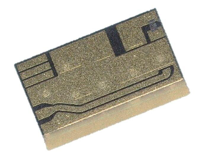
Metallization can also be applied to the sides of a ceramic substrate. This allows multiple surfaces to be electrically connected, enhancing the ground connection.
Example: Submounts for fiber-optic communication.
Thick Cu Metallization
After thin-film processing, thick Cu plating can be applied to support higher current requirements and improve thermal dissipation from devices such as laser diodes.
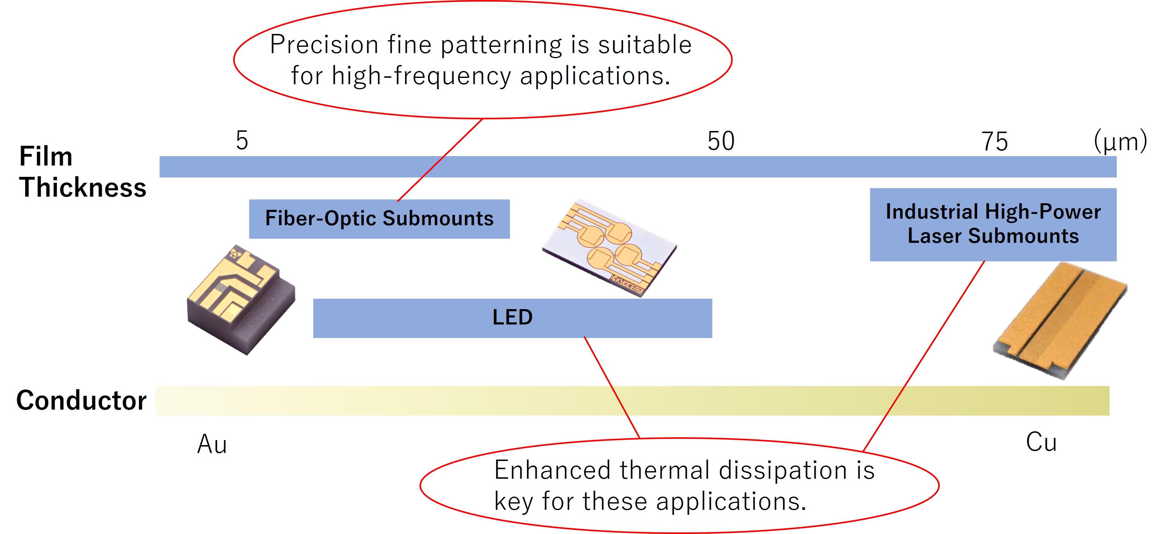
Examples: Film Thickness and Applications
The illustration below shows the optimal film thickness to support different applications and performance requirements.
Kyocera can propose an optimal combination of materials and thin films to support your specific packaging needs.