
Material Selection Influences Performance
In the development of electronic devices, achieving objectives often depends on selecting the right package material. Available in a variety of formulations, Kyocera's ceramics contribute to the development of electronic devices by meeting demanding specifications and enabling new levels of performance.
Examples of Packaging Materials
Imaging Sensors
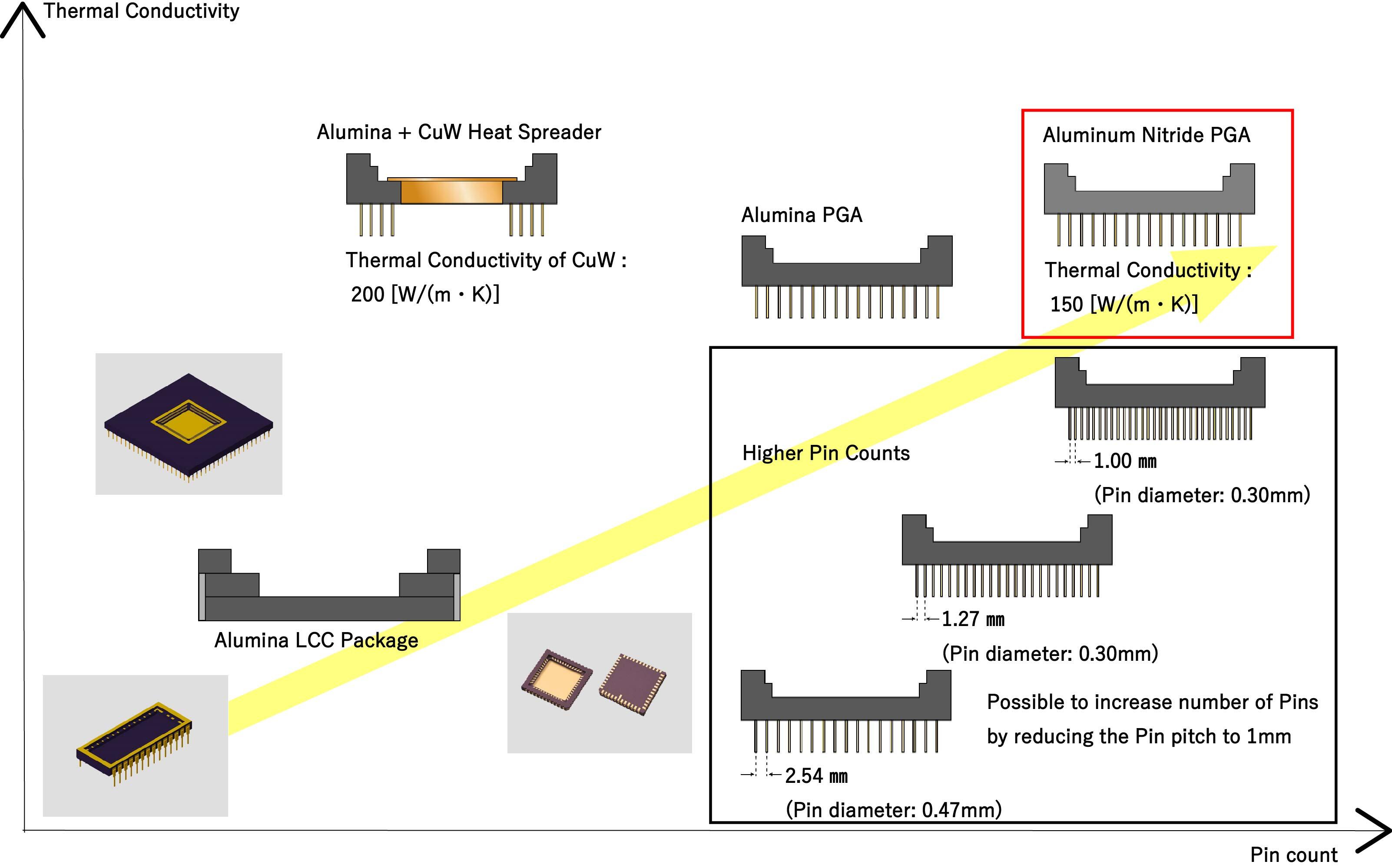
The chart above shows an example of a package proposal addressing heat generation and chip size. For devices with higher heat generation, Kyocera proposes packages with heat spreaders or aluminum nitride material, which offers exceptionally higher thermal conductivity.
As device size increases, Kyocera proposes packages with pins to ensure board-level reliability. Kyocera designs packaging solutions for a wide range of microelectronic applications. Expertise gained by serving many different markets allows us to offer design options tailored to specific product applications and requirements.