Ceramic Packages for Image Sensors

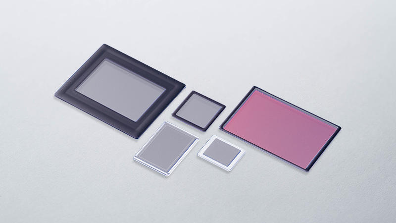
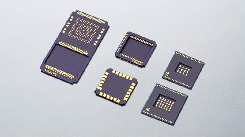
Image sensors are widely deployed in cameras, smartphones, PCs, automobiles, drones, machine vision, and factory automation. When higher performance and reliability are required, image sensors are packaged in ceramics due to the material's superior rigidity, thermal dissipation, structural integrity (with no shedding of microparticles or fibers), and better structural design options.
Features


Characteristics of Ceramics
- Higher thermal conductivity compared to organic materials, enabling more effective thermal dissipation.
- Lower thermal deformation compared to organic materials, enhancing long-term reliability (from assembly to field operation).
- Optional hermetic sealing to protect image sensors from humidity and moisture.
- Ceramics do not shed microparticles or fibers (unlike organic materials), avoiding dust-related yield loss during assembly and field operation.
Benefits of Ceramic Packages
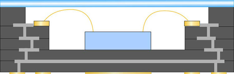
- Created from multiple thin ceramic layers, a ceramic package can be produced with customized structures, including 3-D electrical routing.
- A wire-bonding shelf built into the package improves sensing characteristics by allowing shorter bond wires.
- Ceramic’s Coefficient of Thermal Expansion (CTE) is closer to that of Si, the most common device material, which improves reliability by reducing thermal mismatch during assembly and field operation.
- Higher flexural strength allows thinner material, resulting in lower-profile devices.
Ceramic Packages Support Larger Sensors/ICs That Generate More Heat
One challenge in designing large, industrial image sensors is to match the chip’s CTE as closely as possible with that of the package; and, since larger elements generate more heat, the package material must offer higher thermal dissipation.
Coefficient of Thermal Expansion
Because ceramics offer a CTE close to that of the chip (usually Si), a ceramic package will enhance reliability by reducing thermal deformation over the lifetime of the device, from assembly to field operation.
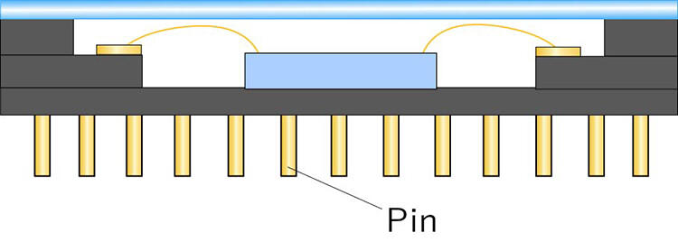
In applications requiring higher board-level reliability, a ceramic package with leads or pins is an effective solution.
Thermal Conductivity
Alumina, a widely used ceramic package material, provides higher thermal conductivity than organic materials, allowing heat from the device to be dissipated more efficiently.
Aluminum nitride offers CTE closest to Si among all ceramic materials, as well as higher thermal conductivity.
In addition, ceramic packages allow a TEC (Thermo-Electric Cooler, or Peltier elements) to be added for enhanced thermal dissipation, along with a metallized seal ring to hermetically seal the device against moisture condensation inside the package.