Challenge 1: Secure Enough Space for Chip Functionality
Challenge 2: Improve Wirebond Process
Devices such as crystal oscillators function through chip vibration, which requires a hollow structure inside the package to provide open space. A cavity structure also facilitates hermetic sealing using a flat lid. Additionally, having a wire-bond shelf inside the package can improve the wirebond process. This page explains the advantages of cavity structures and how cavities are easily created inside ceramic packages.
Advantages of Cavity Structures
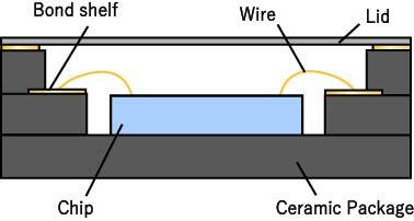
- Cavity structures can be created for crystal oscillators, MEMS chips, and other devices that require space inside the package.
- Lid can be seam-welded.
- Good workability compared to cup-shaped lids.
- Shelf enhances wire-bondability.
- Shelf enables shorter bond wires, which:
- - Improves electrical characteristics.
- - Reduces material cost.
- The cavity structure reduces dielectric loss, since air has a lower dielectric constant than resin.
* Click here for details about hermetic sealing.
How a cavity structure is made
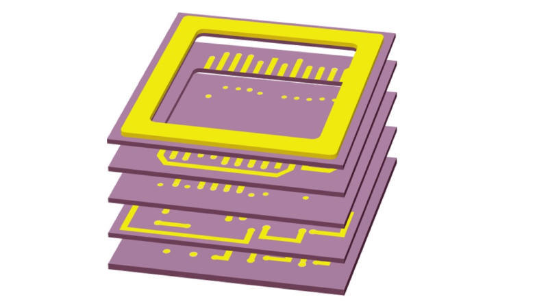
Ceramic packages can be created in multilayer structures that include three-dimensional electronic circuitry, with all layers stacked and co-fired together. A pre-fired ceramic sheet is soft and easy to process, so cavity structures can be formed easily by laminating sheets that have had the cavity space punched out in precise dimensions.
Click here to see the manufacturing process