Challenge: Designing Optimized RF Transmission Lines
In developing high-frequency devices, ceramic packages, FPCs (Flexible Printed Circuits), and PCBs (Printed Circuit Boards) must be tailored to the specific requirements and critical features. Kyocera's expertise in RF transmission line design provides solutions to your most demanding challenges.
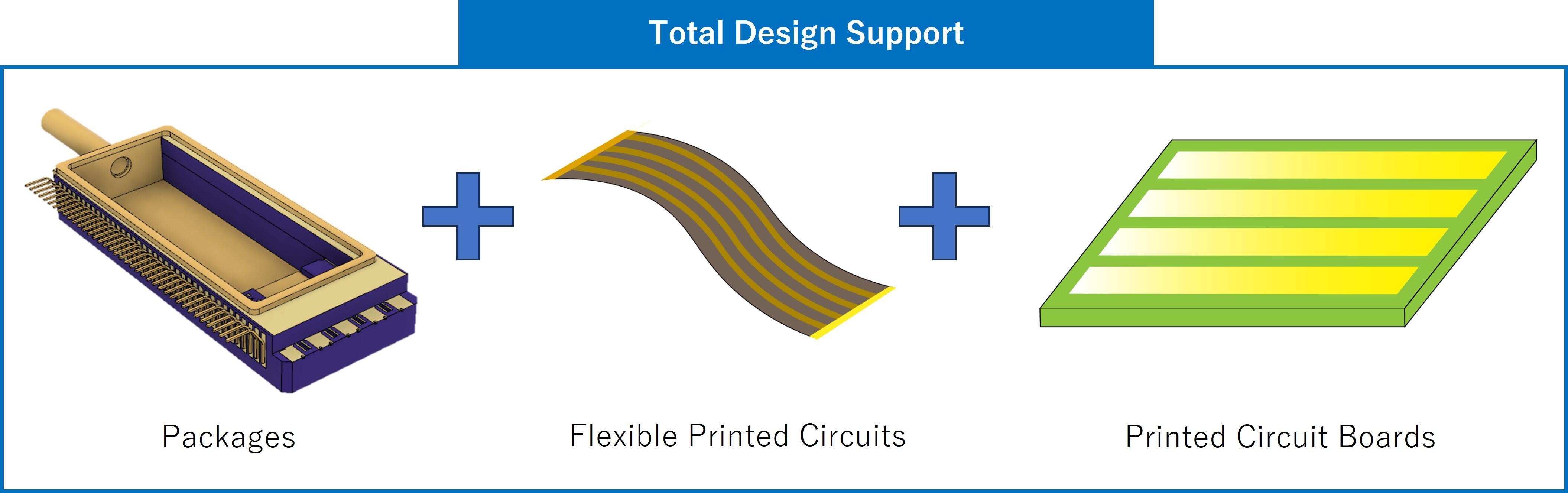
Total Support to Optimize RF Transmission Line Design
Designing packages separately from FPCs and/or PCBs introduces challenges. Kyocera takes FPC/PCB materials, trace routing, assembly layout, and impedance matching into consideration, then factors these variables into a design tailored to the customer's requirements. In addition, Kyocera provides measurement and simulation support above 100 GHz.
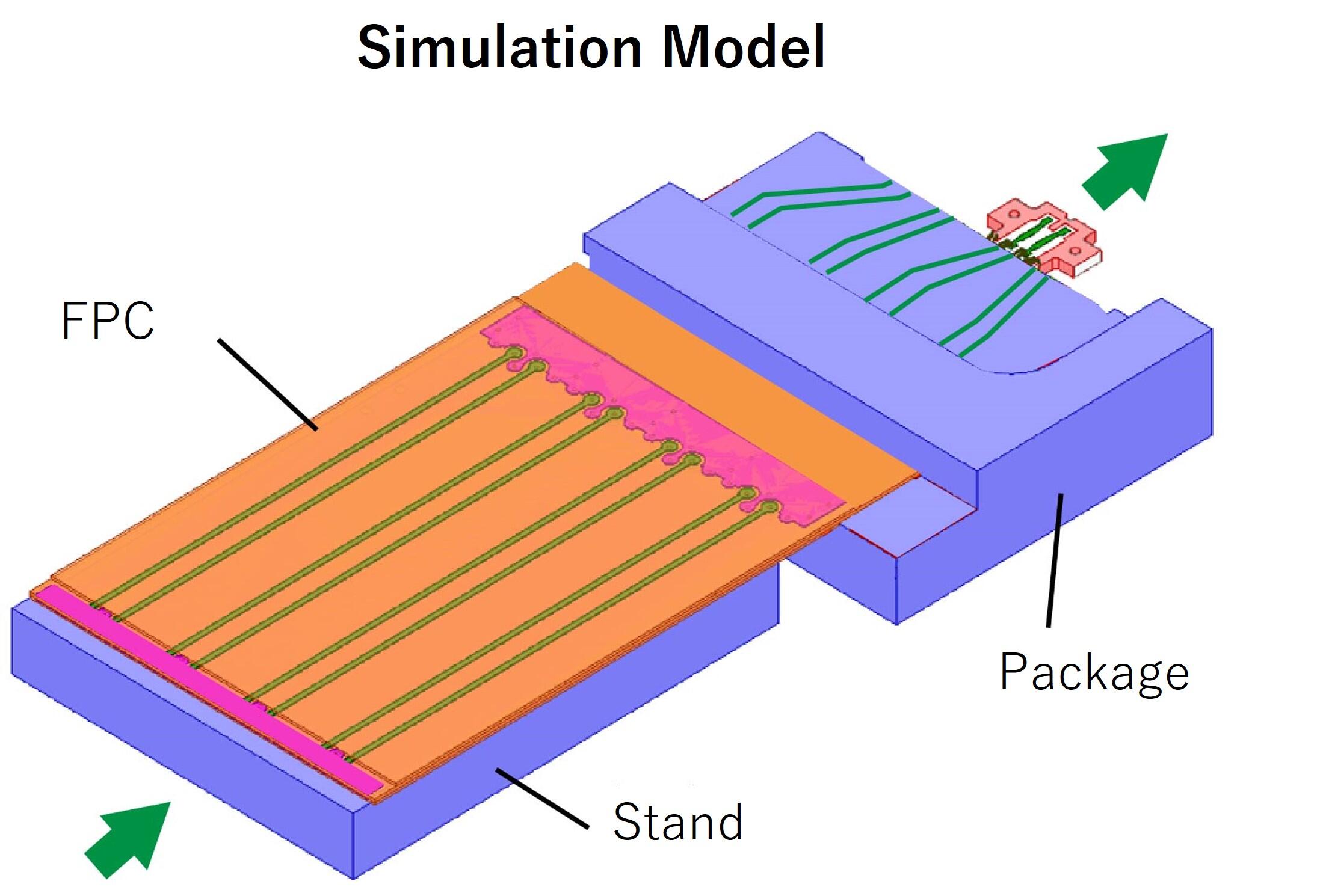
Example: Total Design Support for an Optical Transmission Package
Comparison of Simulation and Test Measurement Data
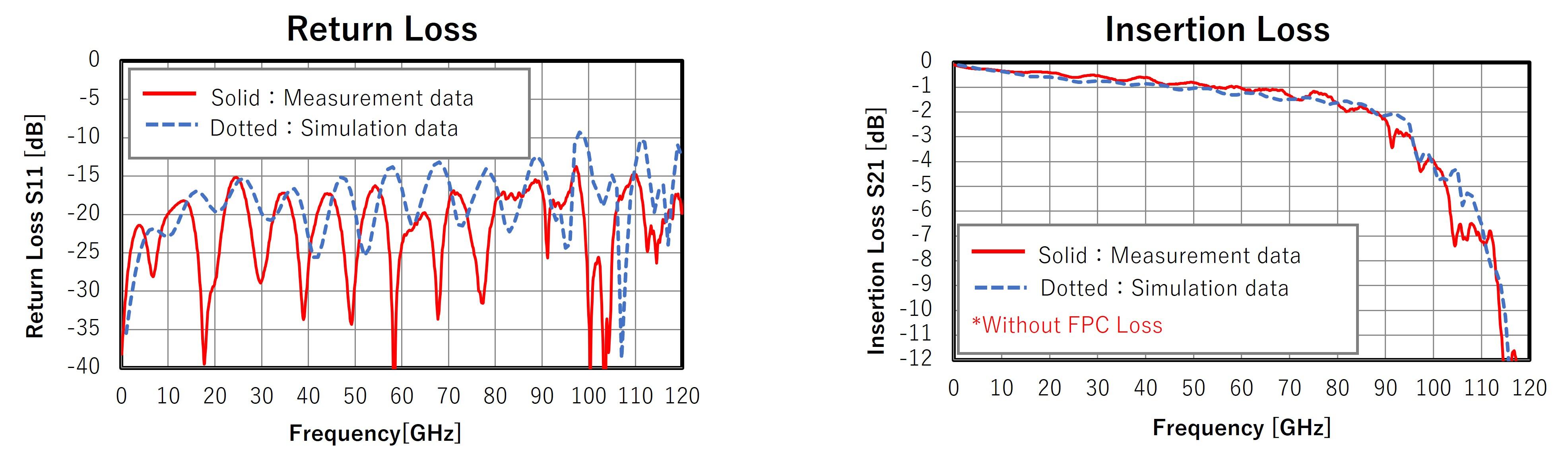
- Kyocera has deep expertise in integrating simulation and test measurement data to deliver optimal designs.
- Kyocera's simulators and network analyzers can model and measure DC ~ 120GHz (over 110GHz are reference values).
- When the measurement data of the products are not sufficient, Kyocera provides the following support:
- Troubleshoot the current product through verification testing.
- Identify negative factors by replicating customer's operating conditions and propose design optimization
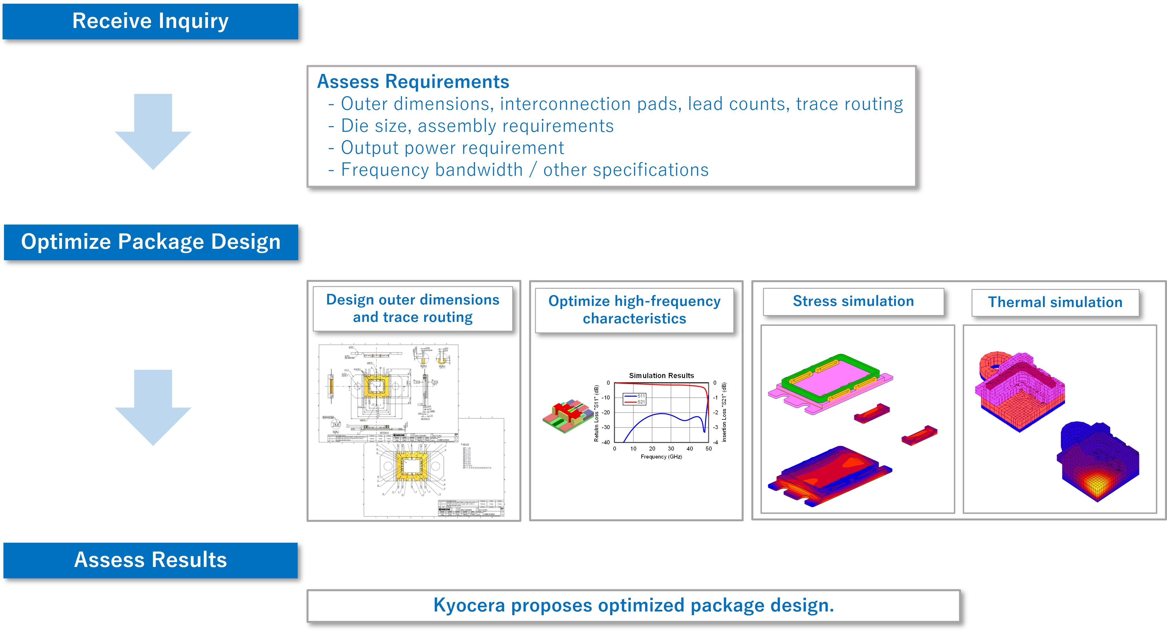
Design Flow