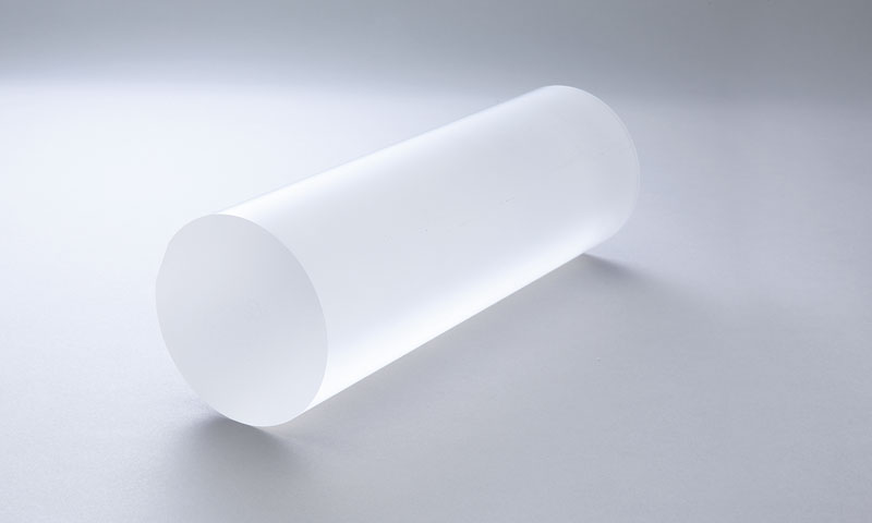
By installing large equipment and improving the structure inside the furnace, Kyocera utilizes the single-crystal sapphire manufacturing technology that we have accumulated over the past 50 years to achieve material growth, grinding, and polishing of large sapphires.
Features
- Manufacturing of extra large products
We can provide square plate products up to 500 mm2 (a plane) and round plate products up to Φ200mm (c plane).
*For details, refer to the design guide below. - Support from growth to product completion
In addition to material growth for large sapphires, Kyocera possesses large-scale equipment and technology for grinding and polishing processes. We can also support commercialization. - Precision processing technology
We can achieve sapphire orientation control with a tolerance of ±0.1°, even for large products.
*The orientation tolerance is based on a partial measurement.
Design Guidelines
Maximum Size for each Product
〔Unit mm〕
| Square Plate Products | |||
|---|---|---|---|
| Orientation | a plane | c plane | r plane |
| Outside Dimension | 500sq. | 200sq. | 500sq. |
| Thickness | 5 | 10 | 5 |
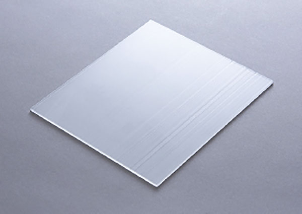
Square plate product example
〔Unit mm〕
| Round Plate Products | |||
|---|---|---|---|
| Orientation | a plane | c plane | r plane |
| Outside Diameter | Φ500 | Φ200 | Φ500 |
| Thickness | 10 | 10 | 10 |
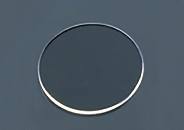
Round plate product example
Processing
Within the above sizes, Kyocera supports full-surface grinding, single- and double-sided mirror polishing, and ring-shaped and complex-shaped products.
*Please contact us regarding sizes that can be processed for each shape.
Surface Orientation Control
tolerance: ±0.1°
Surface orientation: a plane, c plane, r plane
*The surface orientation tolerance is based on a partial measurement.
*Please contact us for information on other sapphire orientations.
Wafer Standard Specifications
Size
〔Unit mm〕
| Size (inches) | Diameter | Thickness | Orientation Flat Length |
|---|---|---|---|
| 2 | Φ50.8±0.25 | (unspecified) ±0.025 | 16±3 |
| 3 | Φ76.2±0.25 | (unspecified) ±0.025 | 22±3 |
| 4 | Φ100±0.25 | (unspecified) ±0.025 | 32.5±3 |
| 5 | Φ125±0.25 | (unspecified) ±0.025 | 42.5±3 |
| 6 | Φ150±0.25 | (unspecified) ±0.025 | 57.5±3 |
| 8 | Φ200±0.25 | (unspecified) ±0.025 | 57.5±3 |
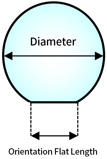
Shape: Compliant with SEMI standard; square shapes can also be supported
Crystal orientation: c plane, a plane, r plane, m plane, etc.; off-angle can also be supported.
Surface Finish
| Surface Roughness (Ra) | Ground | Polished |
|---|---|---|
| Surface | ≦1.2㎛ | ≦0.3nm |
| Back Surface | ≦1.2㎛ | ≦0.3nm |
*Numerical values are reference values, not guaranteed values.
*Please feel free to contact us for information on shapes and specifications other than those listed above.
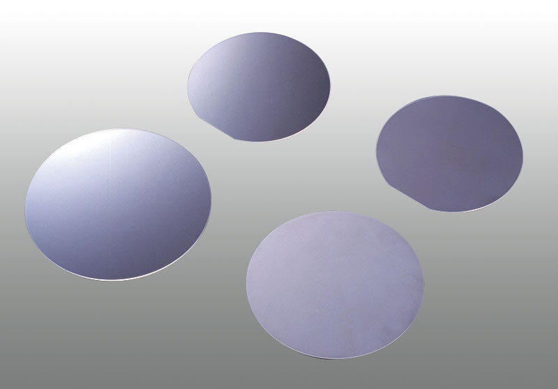
Sapphire Wafers
Processing examples
Kyocera has a track record of processing products such as a large φ450 mm size plate (left photograph) for which X-ray diffraction equipment is used to control orientation, a large ring (center photo), which was bored by machining, and a deposition substrate that was mirror polished by CMP (right photo).
-
Large plate
(whole surface grinding)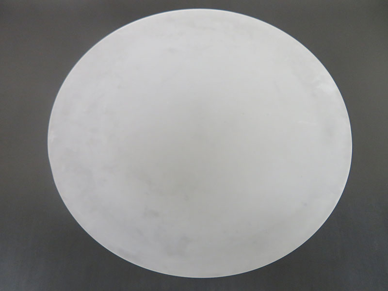
Φ450×5T(mm)
-
Large ring
(ring shaped)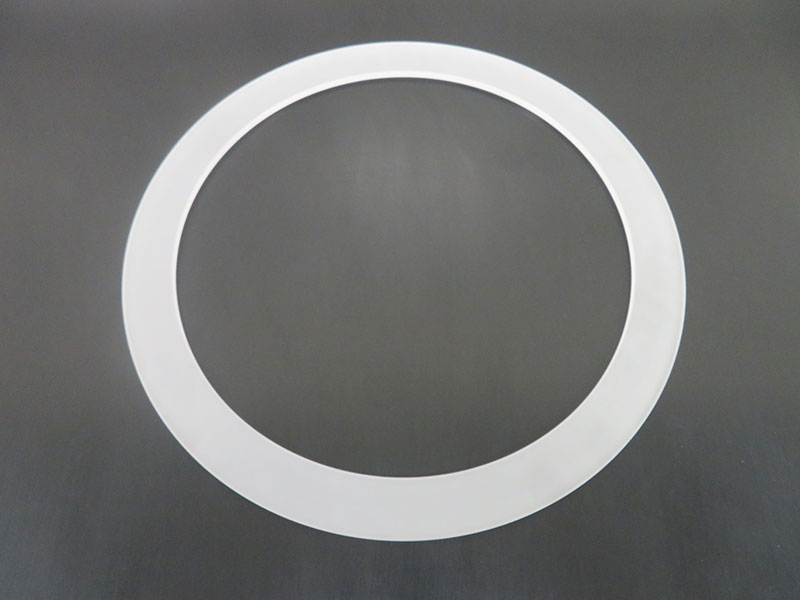
Φ320×φ300×7T(mm)
-
Deposition substrate
(mirror polished on both sides)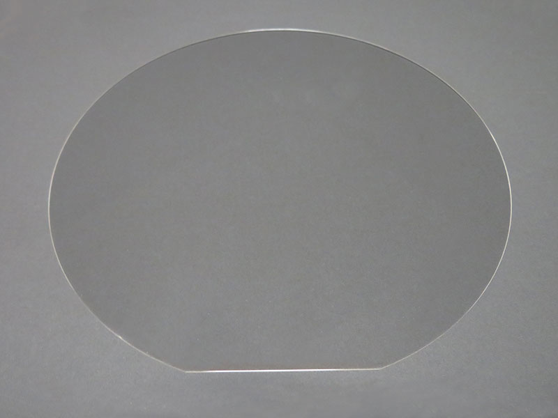
Φ200×0.725T(mm)
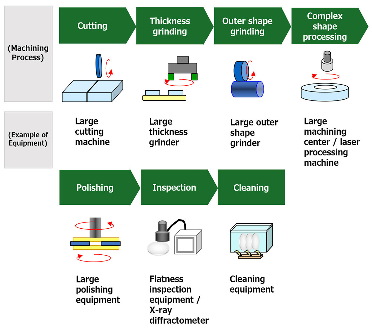
Machining Process
This is an example of the machining process and equipment for large single-crystal sapphire products.
Kyocera possesses dedicated equipment for large-sized products. Through our technical capabilities that utilize our equipment, we pursue product manufacturing that meets the needs of our customers.
All values listed on this page are representative values obtained from in-house measurements,
and do not constitute guaranteed product specifications.
