


Product Search by Industries
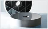
Thick Film Substrates
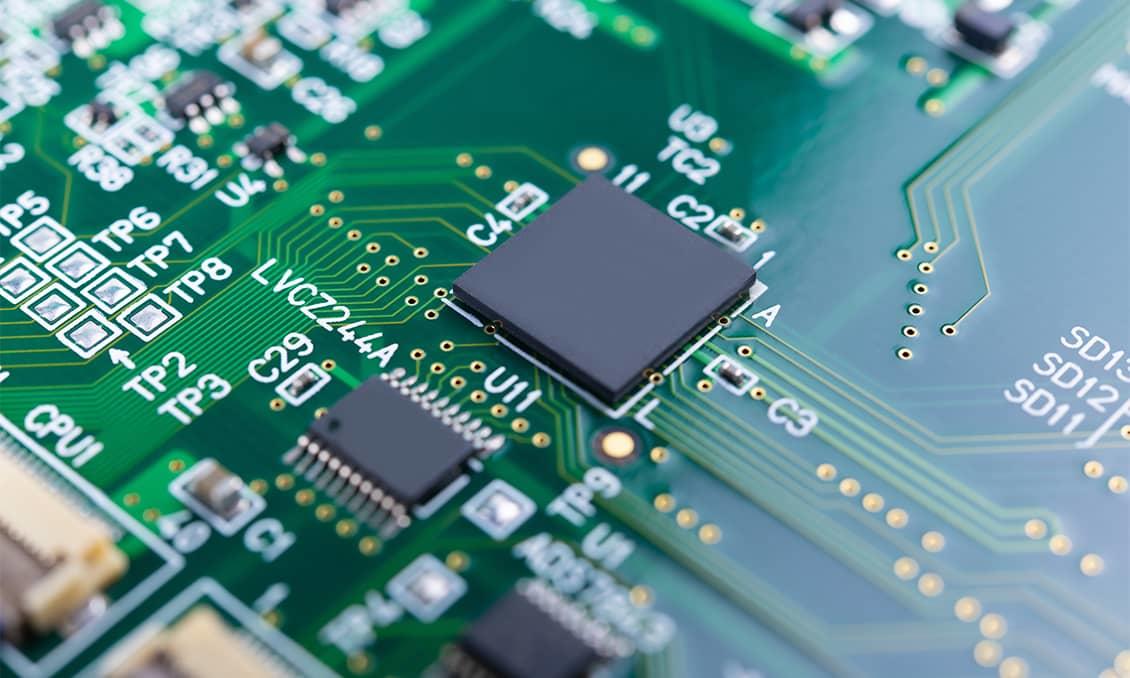
Kyocera's thick film substrates correspond to the increased density and precision of thick film circuits.
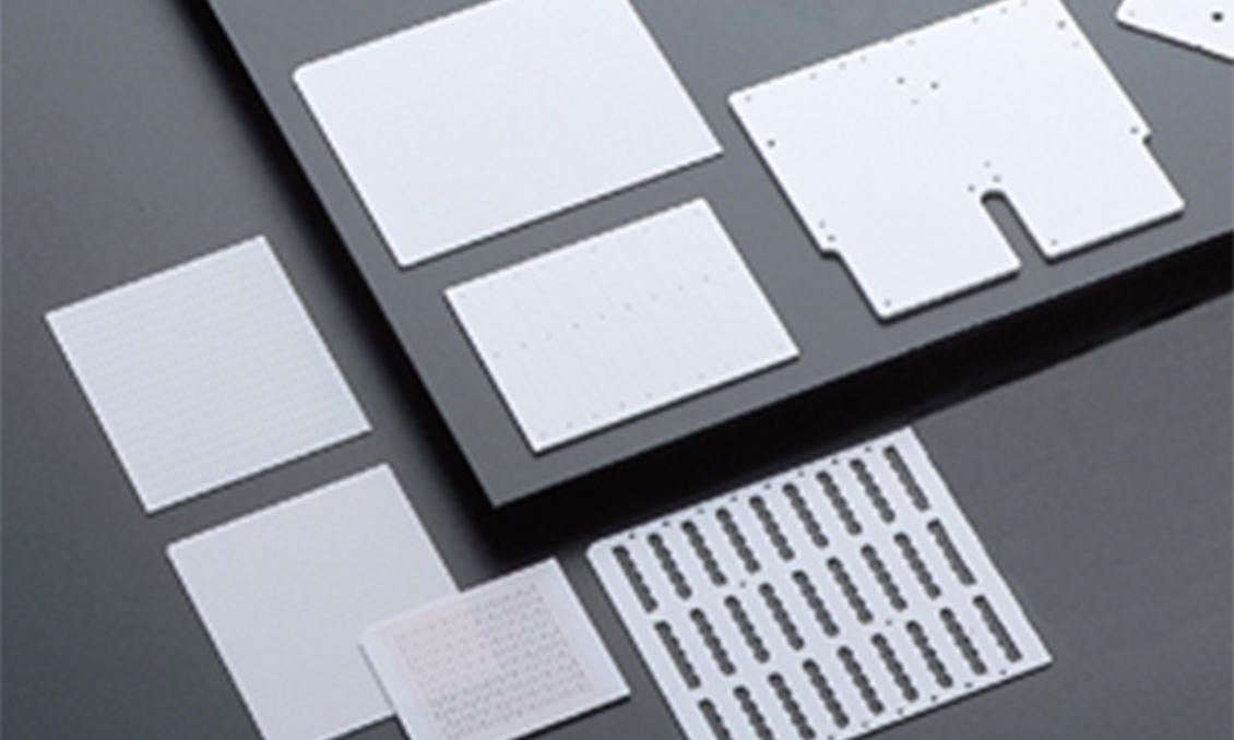
Kyocera produces alumina substrates with excellent thick-film reliability, tightly controlled dimensions (no more than ±0.25%), and small through-holes (as small as 0.2mm), which enable greater density and precision in thick-film circuits.
- Property :
- Large Sizes Available
- Thick Film Reliability
Product Data
| Material | Alumina |
|---|---|
| Size | Maximum Width (mm): 320 (thickness: 0.8-1.0) Maximum Thickness (mm): 3.00 (width 200) Minimum Thickness (mm): 0.32 ( 150 W x 200 L) |
| Precision | Warp 0.2%/inch (W:150 mm x L:200 mm) 0.5%/inch ( 320 mm SQ) |
Applications
- Printed Substrates for Automotive Parts
- Printed Substrates for Sensor Parts
- Printed Substrates for General Thick Film Application