Ceramic Substrates and Packages for Edge-Emitting Lasers

Laser diodes (LDs) experience shorter lifespans when exposed to high temperatures, making thermal management essential. With their excellent thermal conductivity, Kyocera's ceramic packages and submounts help extend the lifespan of laser diodes and ICs while supporting device miniaturization.
Features
Higher Thermal Dissipation
Design Flexibility for Cavity Structures
Surface Mounting

Miniaturization
Hermetic Sealing
Various Thin-Film Options
Higher Thermal Dissipation
Thermally conductive ceramics efficiently dissipate heat generated by LDs and ICs.
Design Flexibility
Ceramic packages offer flexible design options, including surface mounting, miniaturization, and integrating multiple components into a single package.
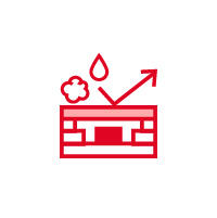
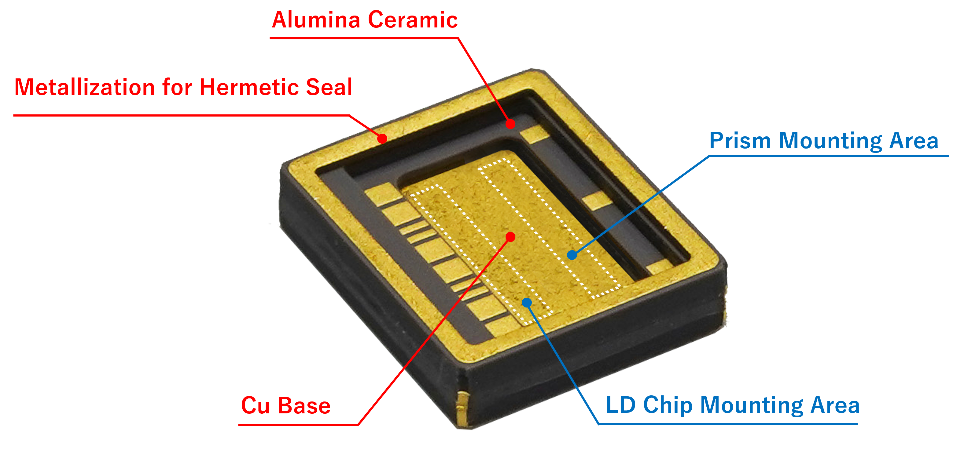
Hermetic Sealing
Laser elements deteriorate when exposed to external environments; ceramic packages can avoid this with hermetic sealing options.
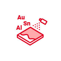
Various Thin-Film Options
Kyocera offers thin films in various configurations customized to meet your requirements.
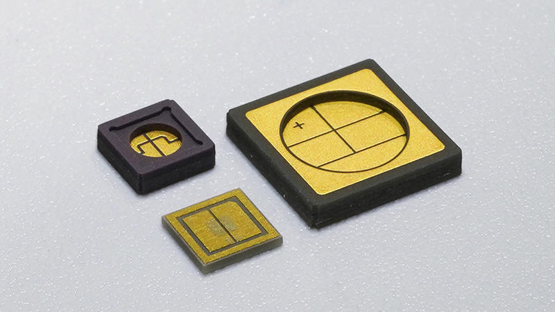
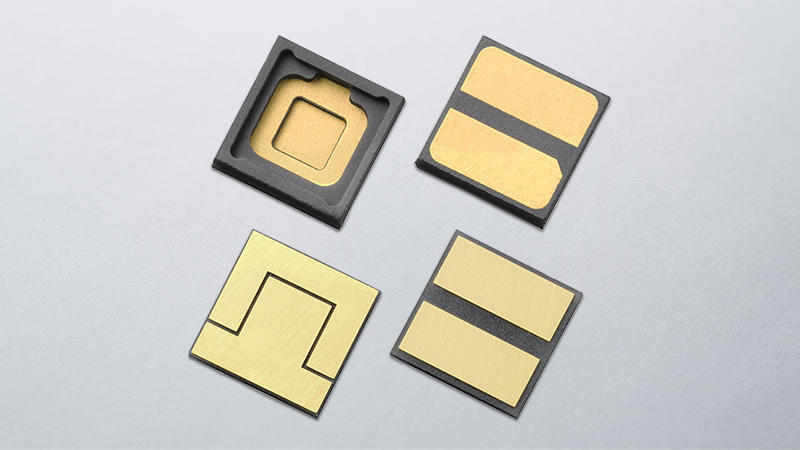
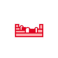
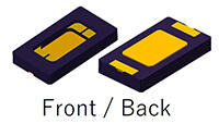
Ceramic Multilayer Packages for Surface Mount Devices
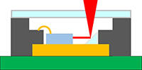
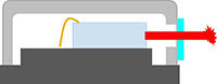
Package Concept for Edge-Emitting Lasers

| Concept | Shape | Image | Cross-Section | Characteristics |
|---|---|---|---|---|
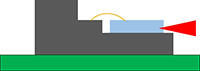
| Shingle Chip | Step (To shorten wire length) | 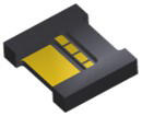 |
 |
|
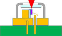
| Can |  |
 |
Compatible with Ceramic Submounts | |
| Bathtub (With Cu Heat Spreader) |
 |
 |
|
|
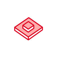
| RGB Module | Convex Shape | 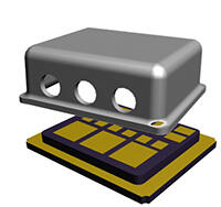 |
 |
|
| Vertical Placement | 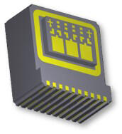 |
|
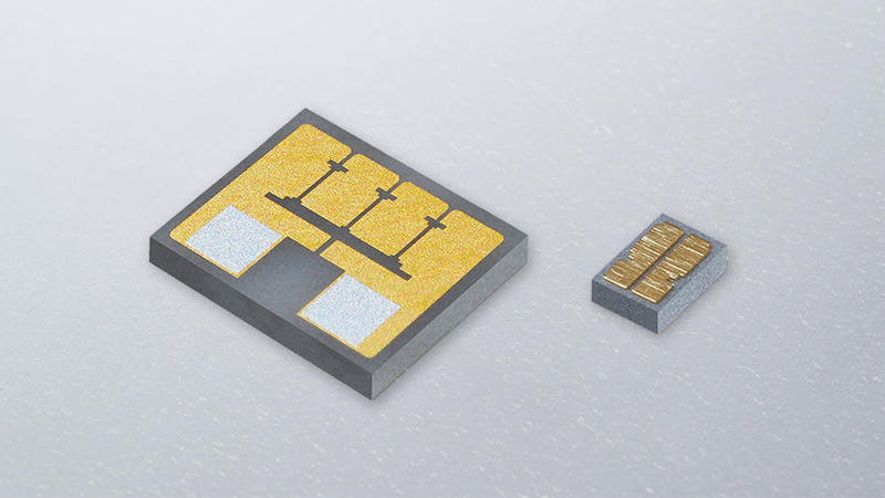
Multi-Chip Mounting
Kyocera’s multilayer ceramics allow multiple components to be integrated into a single package.
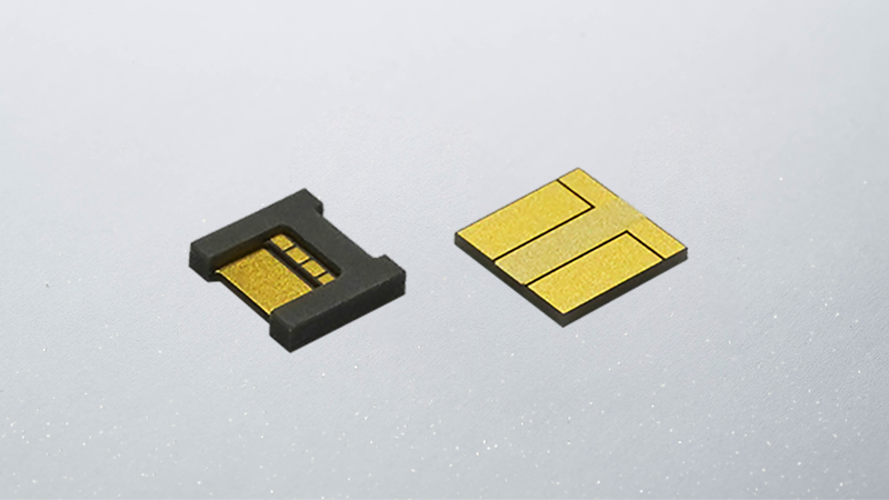
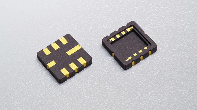
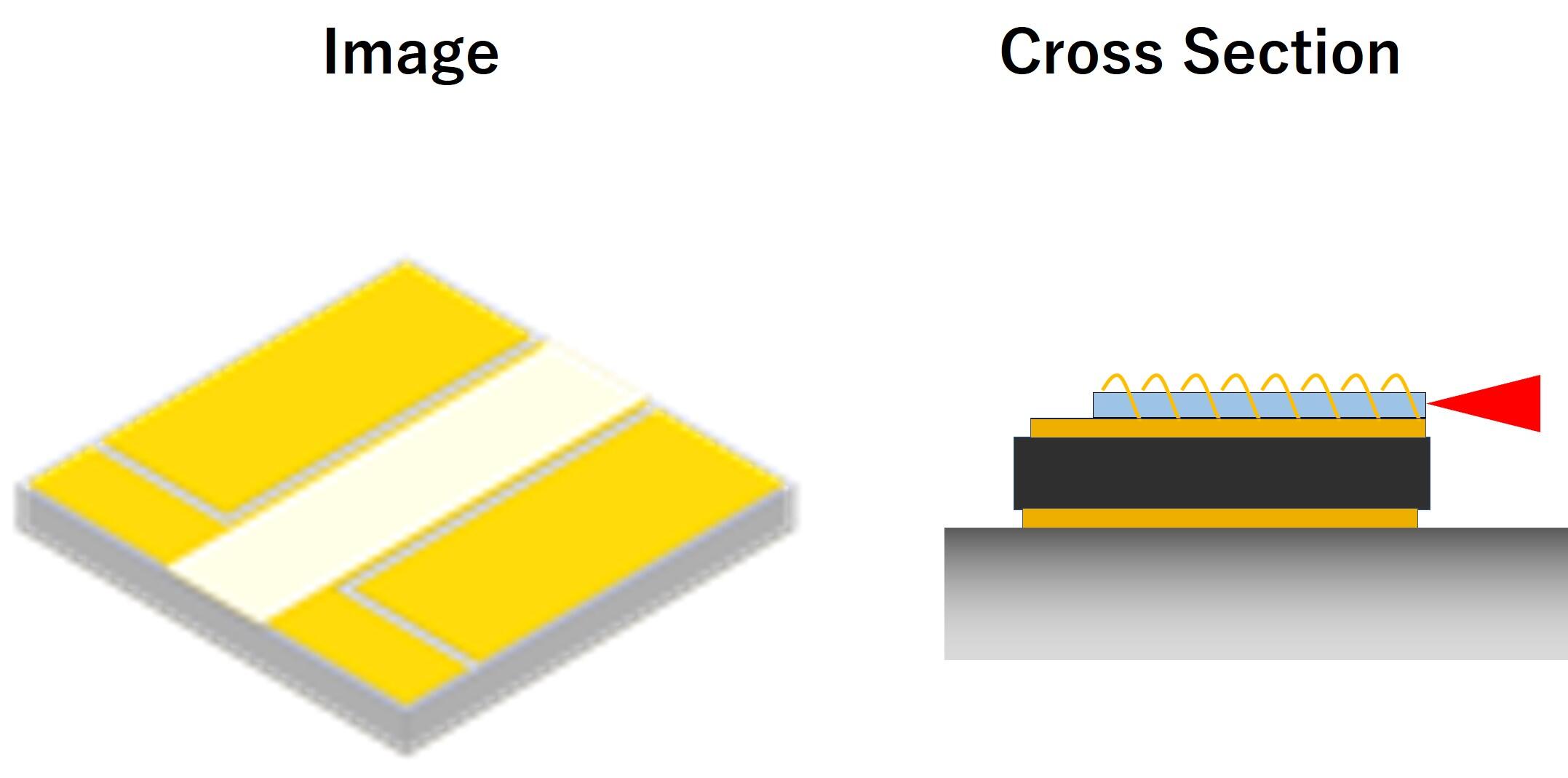
Submount for Laser Diodes
Low Inductance (Low Resistance) Design
Features
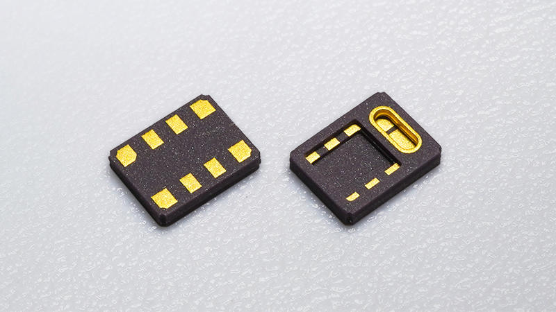
- Film is applied after grinding, ensuring flatness and reducing optical axis deviation.
- AuSn deposition eliminates the need for AuSn preforms during assembly.
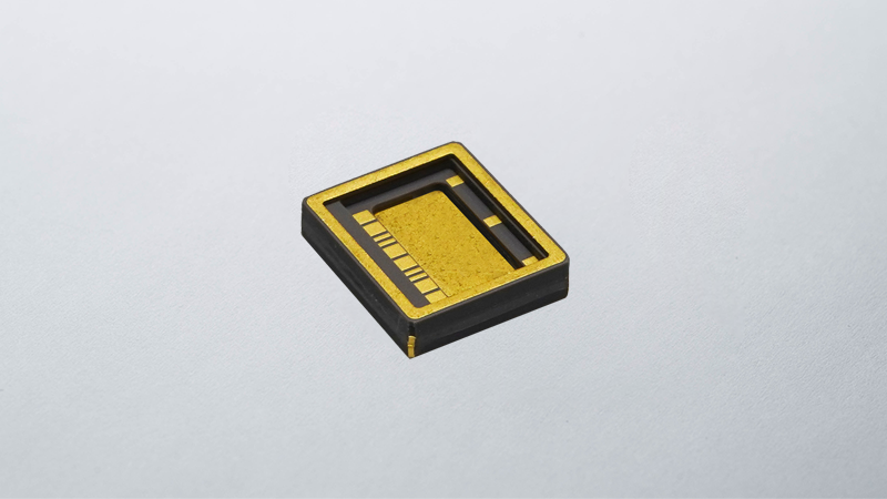
Example: RGB Laser Substrate
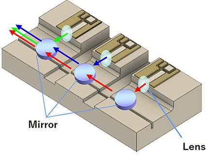
Design includes steps and grooves for lens mounting.
Industrial Laser Submount (Thick Cu Product)
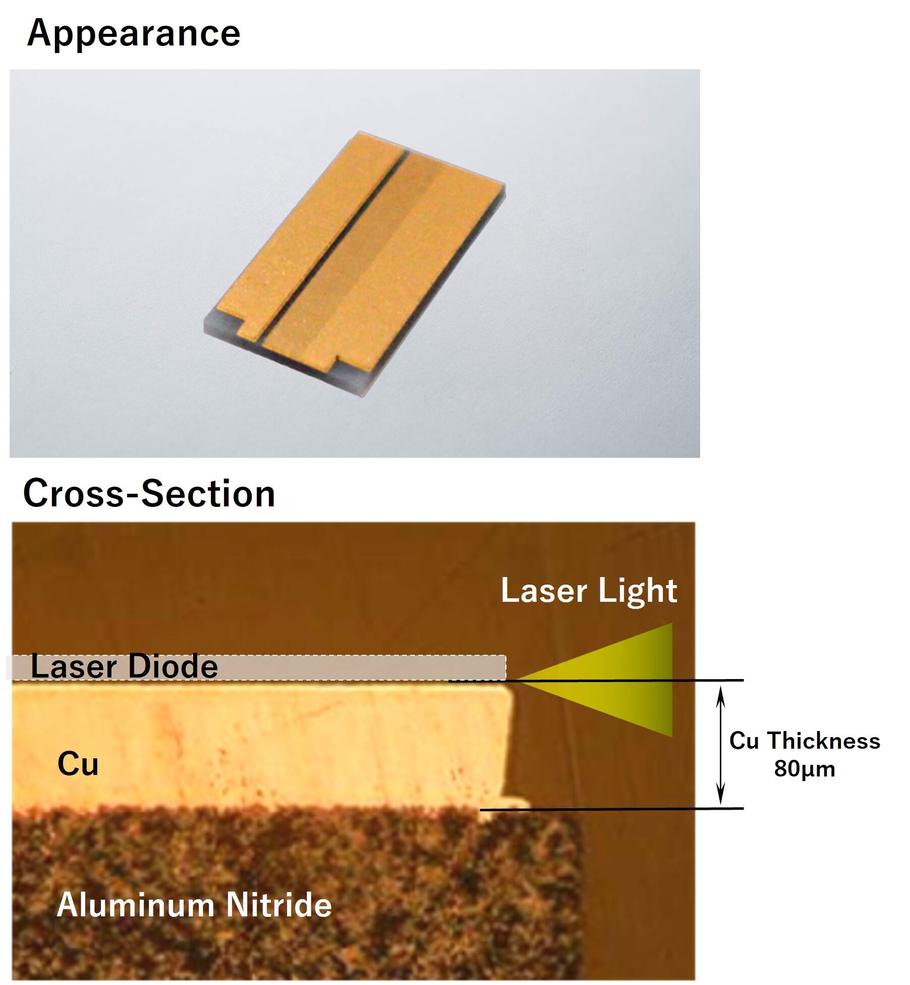
Requirements of Industrial LDs
- Requires high current.
- Must dissipate significant heat.
- Requires high-precision optical alignment.
↓
Kyocera’s Solutions
- Forming a thick Cu layer for thermal dissipation and lower electrical resistance.
- Using AlN substrate material for higher thermal conductivity than alumina.
- Ground and polished thin-film substrate for superior flatness.
FAQ
Materials