Challenge: Miniaturizing Electronic Devices
Smartphones and other electronic products keep delivering better performance and functions. Achieving this without making a product larger is a serious engineering challenge, as circuit complexity and component counts increase continually. The solution lies in miniaturizing electronic devices, such as semiconductors and electronic components. Kyocera is a longtime enabler of miniaturization, developing high-strength materials and improving process technologies to make components both smaller and better.
World's Smallest Ceramic Packages*
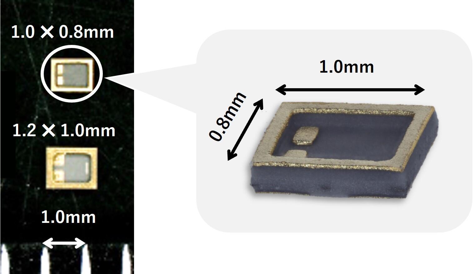
Crystal devices keep getting smaller and smaller. Kyocera has enabled this miniaturization and is taking it to new levels with the world's smallest* (1.0 x 0.8 x 0.17mm) mass-produced ceramic crystal device package.
*Kyocera research (2023)
Technologies to Promote Miniaturization
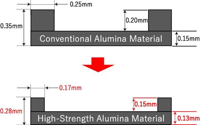
High-Strength Materials
Example: AO700 (flexural strength: 620 MPa)
AO700 is a high-strength alumina material offering flexural strength 1.5 times higher (based on Kyocera's research) than conventional alumina ceramic material. This material is used to create packages smaller than 2.5 x 2.0mm.
High-strength alumina: click here for details
2.0mm x 1.6mm package concept
Kyocera's ultra high-strength materials allow packages with thinner walls and bottom layers to withstand the mechanical stress of the sealing process. This illustration indicates how the cavity area can be increased without changing the overall package size.
Process Technology
Process Accuracy
Miniaturizing ceramic packages requires ultra-precise manufacturing technologies, including a high-accuracy seal-ring brazing process. Kyocera has successfully mass-produced the world's smallest compact packages through continuous improvement in our manufacturing process technologies.
Flexible Options for Design / Structure

Dual-cavity example for miniaturization
Ceramic packages can be easily designed in 3D structures, allowing designs that fit the widest range of requirements in device count and dimensional specifications. This illustration shows a dual-cavity structure optimizing space efficiency and miniaturization.
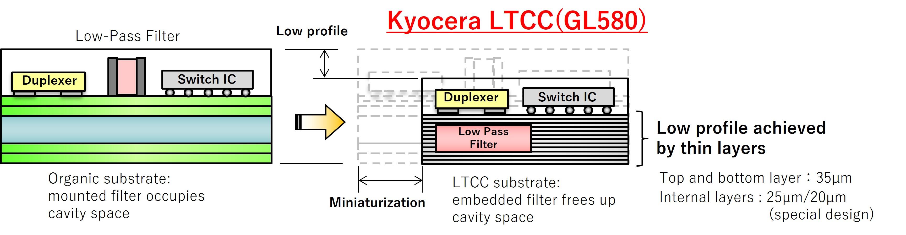
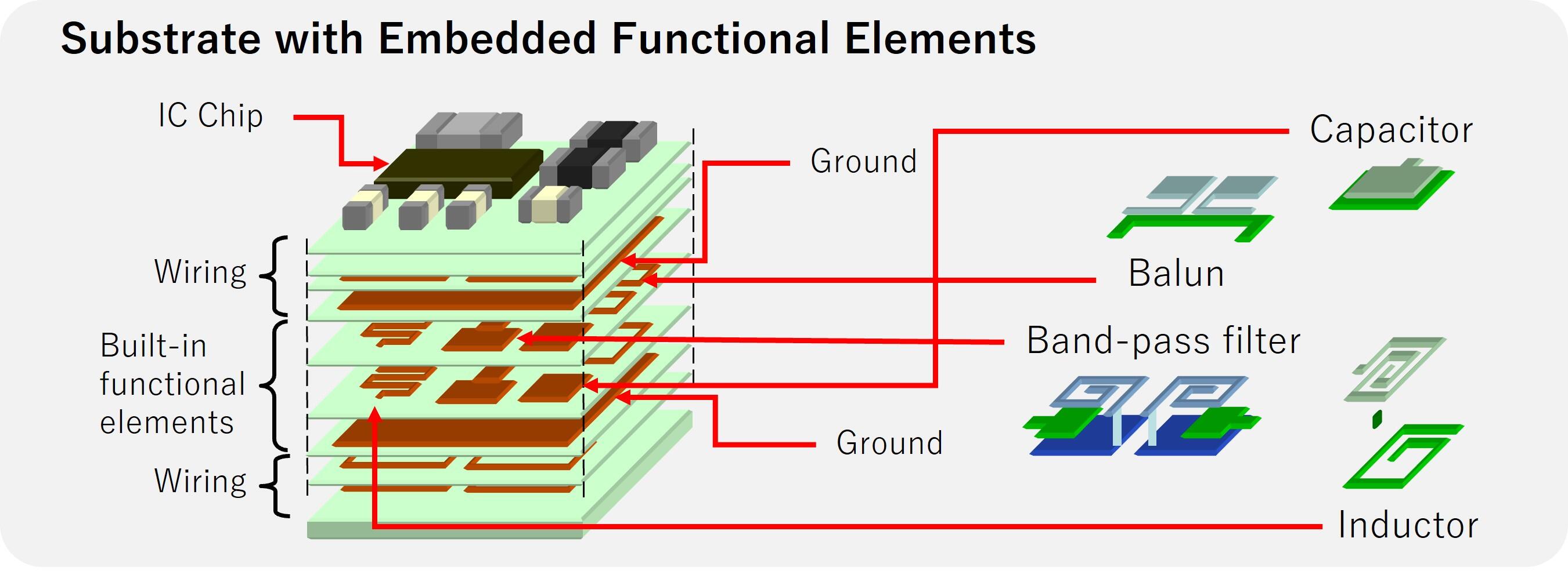
Enhancing Miniaturization: LTCC Materials with Embedded Functional Elements
Kyocera's LTCC material (GL580) allows capacitors, filters, inductors, and baluns to be created directly within the layers of a ceramic package or substrate. By embedding passive components that would otherwise require extra space, ceramic materials offer another powerful tool for module miniaturization.
Example: RF module with embedded filter