Challenge: Advancing Miniaturization as Component Counts Rise
As smartphones and other electronic products expand in functionality, with more and more components added to ever-denser circuit boards, the need to miniaturize semiconductors and electronic components keeps growing. Thanks to the design flexibility afforded by ceramic packages, design engineers can propose more compact structures that integrate multiple elements, such as sensors and ASICs, into a single package. Kyocera's expertise in ceramic package design and manufacturing provides new levels of miniaturization for demanding requirements.
Examples of Ceramic Package Structures
Examples for Miniaturization
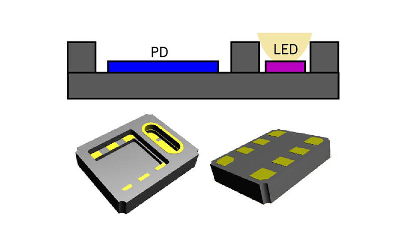
Dual Cavity Structure 1
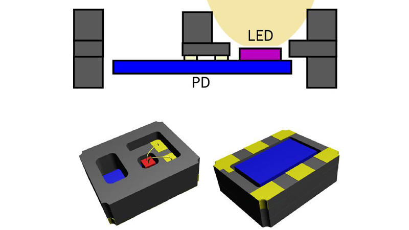
Dual Cavity Structure 2
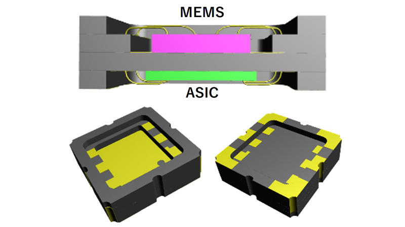
Dual Cavity Structure 3
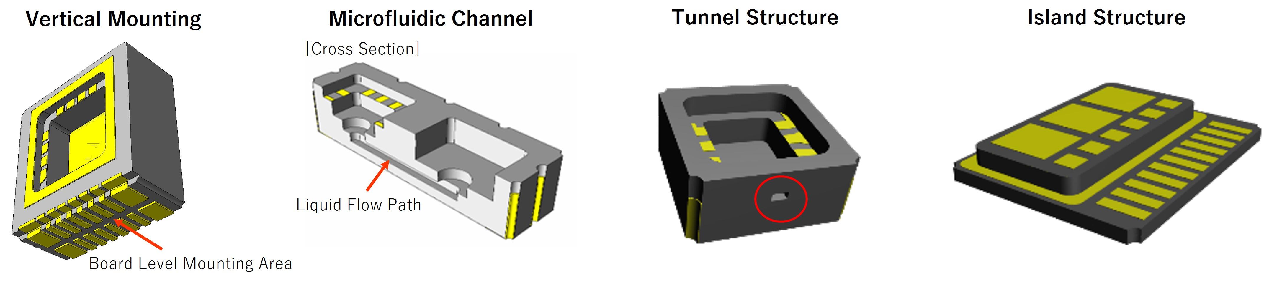
Other Custom Structures
Other Related Solutions
Product Categories
Solutions
Materials