Challenge: Reduce Profile / Miniaturize Electronic Devices
Smartphones and other widely used electronic products are becoming more functional with each new generation. Circuit boards must become increasingly dense to accommodate more components without increasing the size of the smartphone. This makes miniaturization one of the most important trends in electronic devices, including semiconductors and passive components, where lower profiles are in great demand. Kyocera's material technologies, substrates, and packages are essential to making electronic devices both smaller and better.
Thin Multilayer Technology
Ceramic packages are manufactured through a process of via-punching, via-filling, printing, laminating, and firing extremely thin sheets of ceramic. Although making these insulating ceramic sheets thinner is a challenge, Kyocera is continually developing process enhancements to mass-produce thinner and thinner ceramic packages. For SAW device applications, Kyocera is currently mass-producing ceramic substrates just 0.1mm thick.
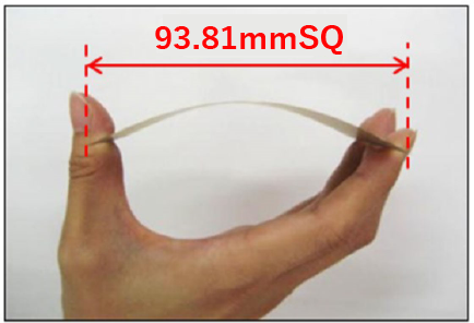
Lower Profile Made Possible by High-Strength Materials
High-rigidity, high-flexural-strength ceramics are essential to making the thinner substrates and narrower walls required to reduce the profile and miniaturize microelectronic device packages.
Click here for details on Kyocera's high-strength AO700 and AO800 ceramics.
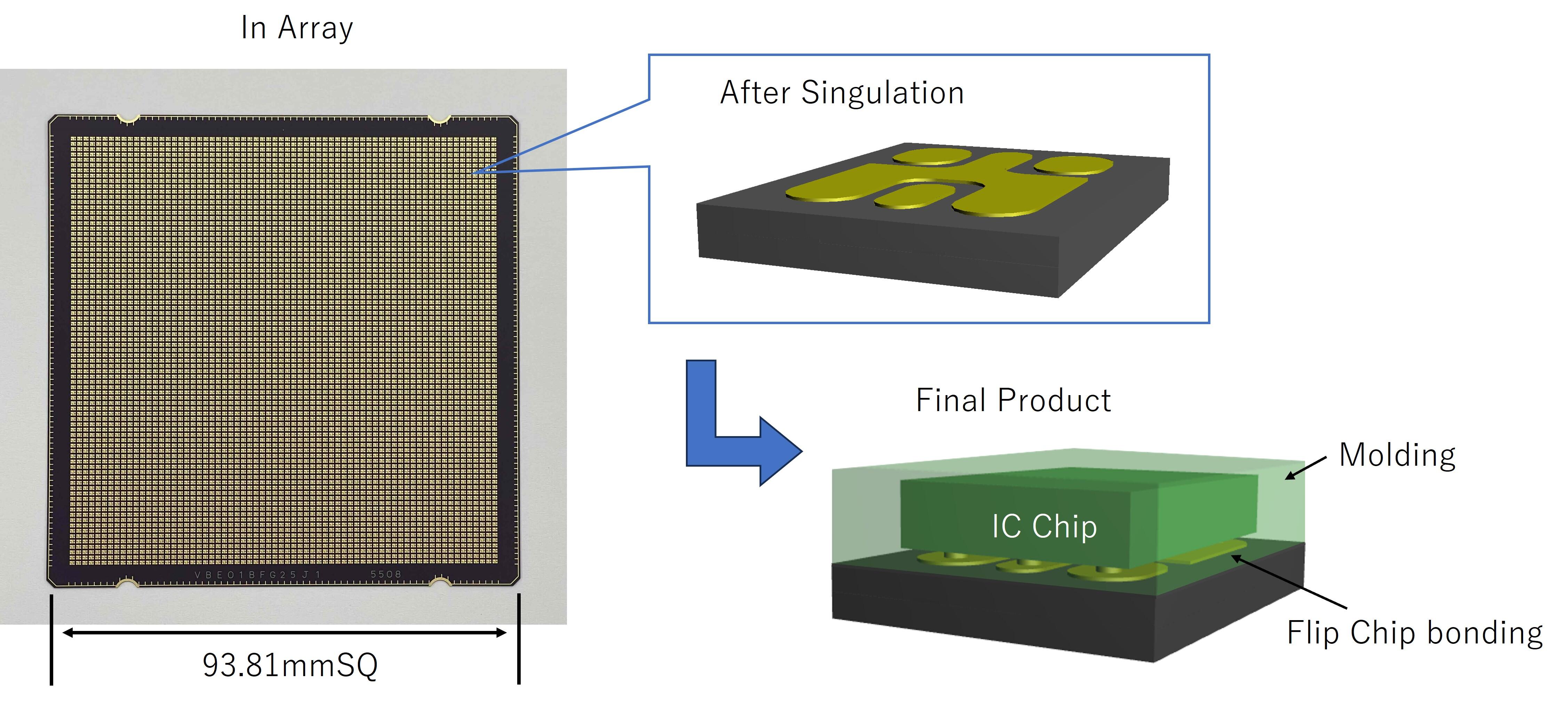
Application Example
CSP Substrate for SAW Devices
Note: CSP - Chip Scale Package
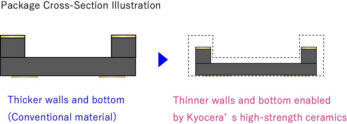
High-Strength Packages for Quartz Devices
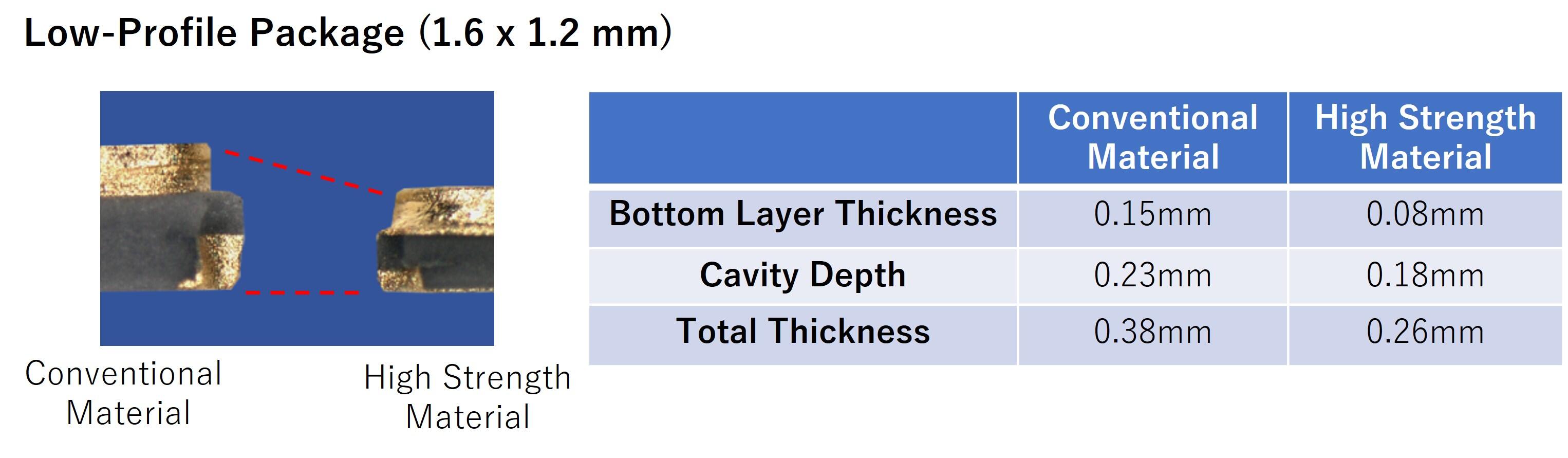
Creating the substrate from high-strength ceramic can allow the thickness of the package to be reduced.
Click here for details on Kyocera's high-strength AO700 and AO800 ceramics.
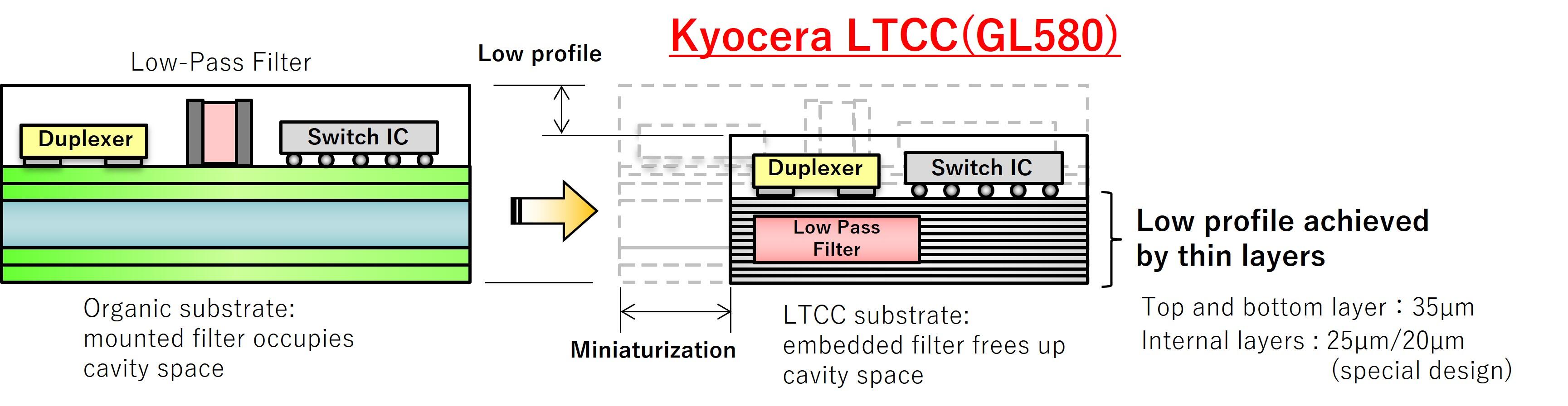
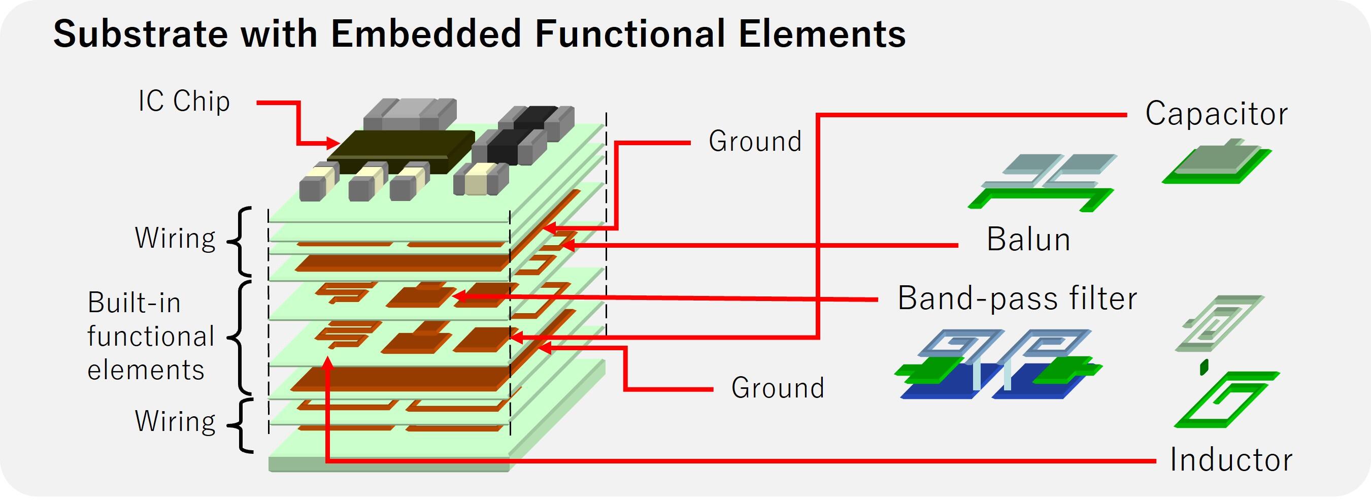
Enhancing Miniaturization: LTCC Materials with Embedded Functional Elements
Kyocera's LTCC material (GL580) allows functional elements, such as capacitors, filters, inductors, and baluns, to be created within the substrate. Kyocera can provide custom solutions for module miniaturization using this capability.
Example: RF module with embedded filter