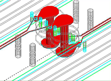
Transmission Line Simulation
By making use of Kyocera’s know-how in high-performance design of printed boards, we provide transmission line simulation for secure transmission of high-speed signals in the gigahertz region. We propose extraction of issues and optimizing at the designs

We identify problems in the design stage and propose optimization through verification of signal integrity including analysis of electric parameters to ensure matching of characteristic impedance, modeling of connector components, and coordinated design including LSI packages or chips.
Main Services
Transient analysis / AC analysis
- Transmission analysis for signal boards and a whole systems
- Optimizing characteristic impedance by TDR analysis
- Inspecting and optimizing margin of time and voltage change
- Optimization while considering a variety of devices and boards
- Eye-pattern analysis for high-speed signals
Device modeling
- Making models from physical figures and properties
- Measurement of S parameter for components and making models
Applications
- Motherboards of high-performance equipment, consumer game machines, medical equipment, automotive equipment, and consumer devices.
- Modeling from S parameter of connectors, etc.
Transient analysis for whole systems
We conduct transient analysis of the whole systems, which allows us to verify and optimize arrangement of wires, routes of return current, constants of “problem-solving” parts, or drive capability without waiting for evaluation of an actual board, reduce the need of reworking, and ultimately make a remarkable reduction in product development period.
Cooperative design of Packages and Motherboards
Development of coordinated design for a package and a board can optimize the buffer capability and signal pin assignment, and optimization of the power source ground pins can reduce the wiring area or the number of layers of a board. These measures ultimately allow us to propose board cost reduction. We can develop optimal design for high-speed wiring, such as DDR memory interfaces and high-speed serial interfaces, and power source systems. We have rich experience in coping with major ASIC/FPGA models.
Eye-pattern analysis of high-speed differential line
We can assess eye-pattern analysis of PCI Express Gen3, USB3.0, XAUI and others, and measure emphasis/equalizing at the design stage. We can implement solid wiring without transmission error.


