EMI / ESD / Thermal Simulation
Design support service that can only be provided to customers by a company who knows everything about the characteristics of printed wiring boards
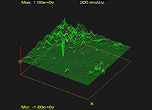
In general, it is difficult to identify the causes of and formulate counter measures for electromagnetic Interference (EMI) in an actual device. We optimize the placement/wiring and return path of power through differential mode emission analysis and common mode emission analysis at the design stage in order to minimize EMI. We also manage analysis of electrostatic discharge (ESD) and thermal analysis.
Main Services
EMI analysis
- Analysis of differential mode emission from signal loop, and optimizing placement, wiring and power plane.
- Analysis of common mode emission from potential difference between signal grounds, and optimizing power plane shapes and bypass capacitors.
ESD analysis
- Optimization of ground beta shapes and capacitors
- Verification of effects that ensures shifting from ESD, such as reset signals, to signals that you want to protect
Thermal analysis
- Optimization of parts arrangement and patterns
- Analysis of heat including casing or fluid analysis for verification of the effects of forced air-cooling by fans or holes provided in the casing
- Capable of being applied to thermal stress analysis
Applications
- Motherboards of high-performance multiple equipment, medical equipment, electronic instruments, and automotive equipment.
EMI analysis
We manage the EMI level of the board by picking out signals which have high-level noise, and optimizing component placement and routing. This can also maintain margin operation of the circuit.
ESD analysis
We construct models based on actual design. Then simulate the discharge noise from outside boards, looking over capacitors effects.
Thermal analysis
We make the thermal distribution visible with thermal components on printed boards. Analysis of thermal distributions on boards including thermal conductive properties of printed boards and thermal distribution with chassis are available.
Optimizing component placement, and optimizing beta pattern which function as heatsink and number of vias on board are available.