High-Layer-Count PWBs
Achieving the sub-lamination structures to Accommodate Smaller Component Pitch
High-layer-count PWBs are used as main boards in a wide range of applications, including information and communications equipment such as servers, routers, switches, and base stations, as well as industrial equipment such as semiconductor manufacturing equipment and measuring instruments.
Kyocera offers high-density, high-layer-count PWBs designed to accommodate the increasingly smaller pitch of mounted components.
Features
- Maximum board thicknesses up to 3.6mm
- We offer high-Tg materials from our extensive lineup.
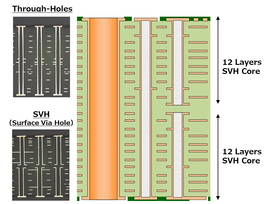
Cross-Section Example
Applications
- Servers
- Semiconductor manufacturing equipment
- Wireless communication base station
- Mesuring instruments
Our Experts can help