Ceramic Packages
for Next Generation XR Displays

Exploring the Metaverse
with XR Technology
Extended Reality (XR), a technology that merges the physical and virtual worlds, is advancing rapidly with promising applications in entertainment, education, medicine, business, and industry.
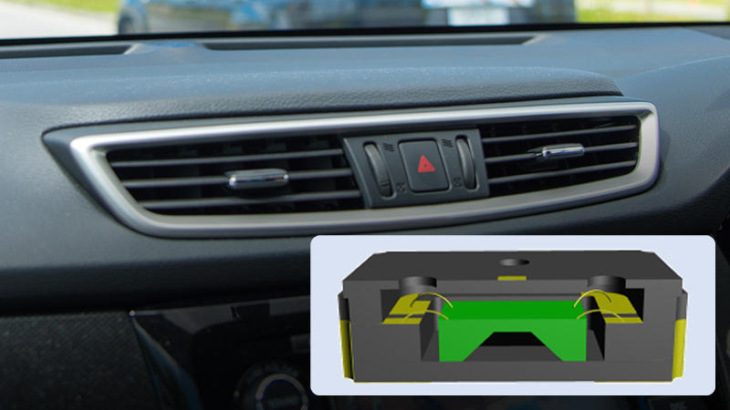
XR devices, such as head-mounted displays (HMDs) and smart glasses, are equipped with a variety of technologies. This page introduces ceramic package technologies for XR displays.
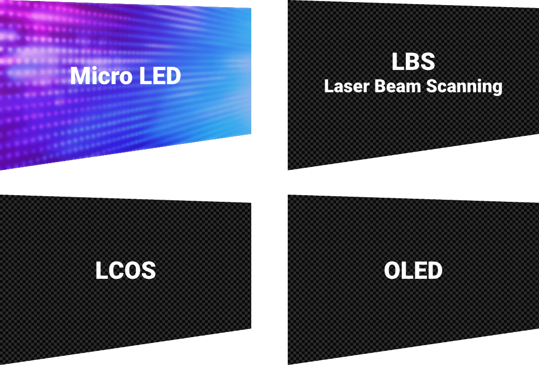
Various display technologies are employed by different XR devices.
Click here for our Tech Blog: Kyocera's Ceramic Packaging Technology Supports XR Device EvolutionXR Display Technologies
Different XR devices incorporate various display technologies, including Micro LED, Laser Beam Scanning (LBS), Liquid Crystal on Silicon (LCOS), and OLED.
What Is Micro LED?
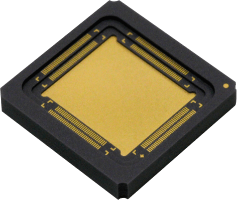
Micro LED is an advanced display technology based on extremely small light-emitting diodes (LEDs). This technology is expected to find widespread use in XR devices because of its excellent brightness, contrast ratio, and image resolution.
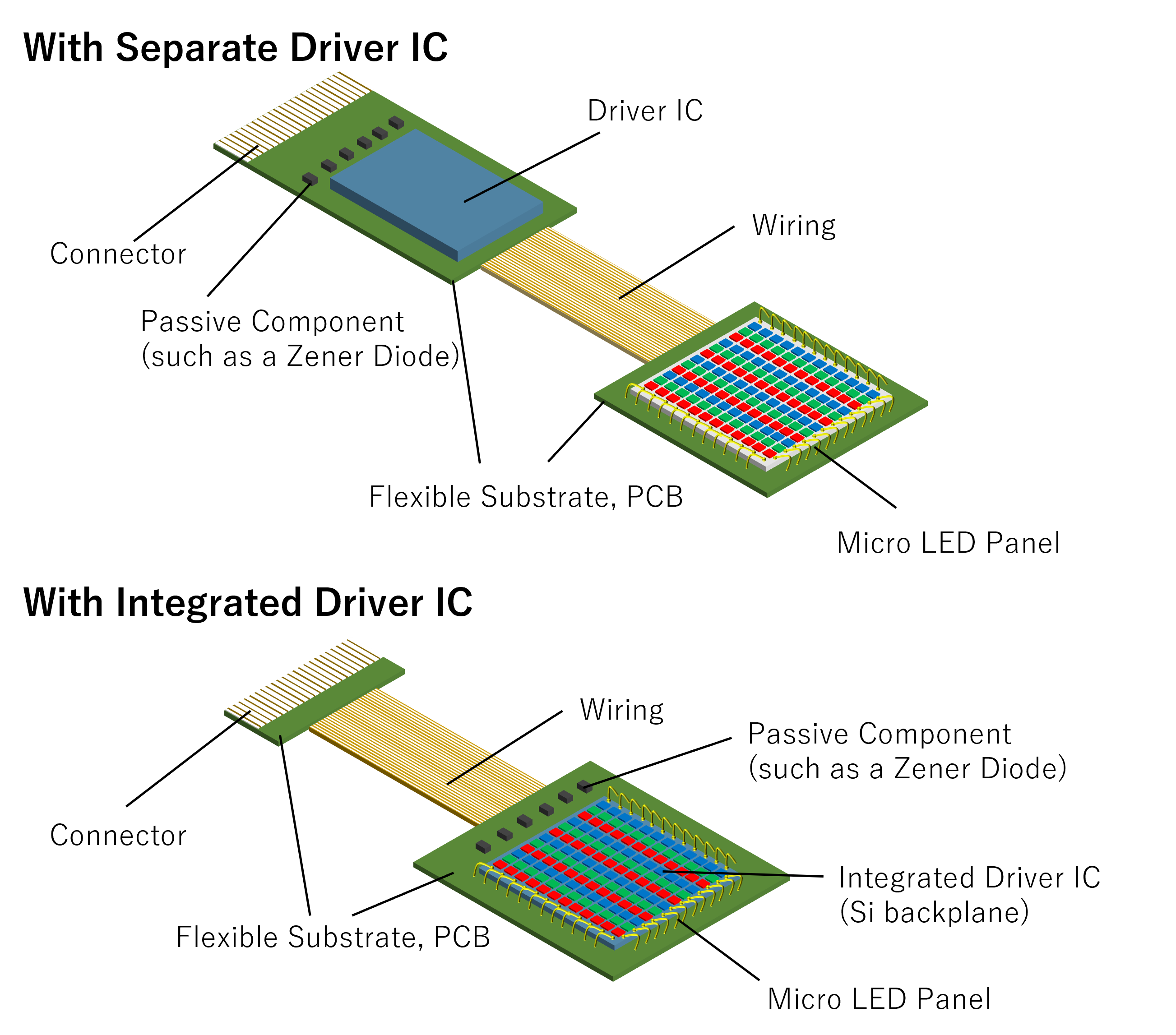
XR devices are generally equipped with Micro LED modules, as illustrated in the right following figure.
While Micro LED modules display excellent, high-resolution images, they also present unique challenges.
Ceramic technologies that can help solve these challenges are explained in the following sections.
Micro LED Module for XR Device

Challenges Encountered by Micro LED Modules
-
Challenge #1
Miniaturization
Micro LED modules must be miniaturized to reduce the size of XR devices
-
Challenge #2
Thermal Management
Heat generated by microelectronic components and drivers must be dissipated efficiently to avoid malfunctions and display failure.
-
Challenge #3
Preventing Light Source Distortion
The light-emission direction of each pixel must be kept constant to ensure high image quality, but heat and other factors can cause deformation that reduces image quality.
-
Challenge #4
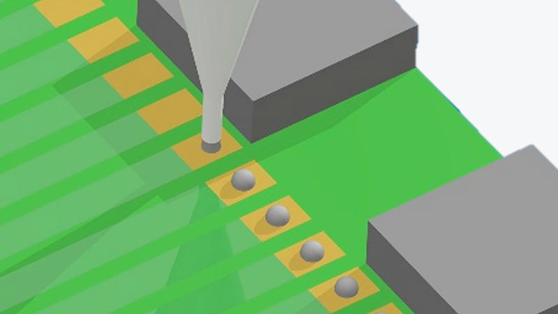
Providing Low-Loss, High-Density Wiring to Ensure Excellent Display Quality
High image quality depends on low-loss, high-density electrical wiring.
Solving the Challenges
of Micro LED Modules:
The Ceramic Package Proposal
Solution to Challenge #1
Miniaturization
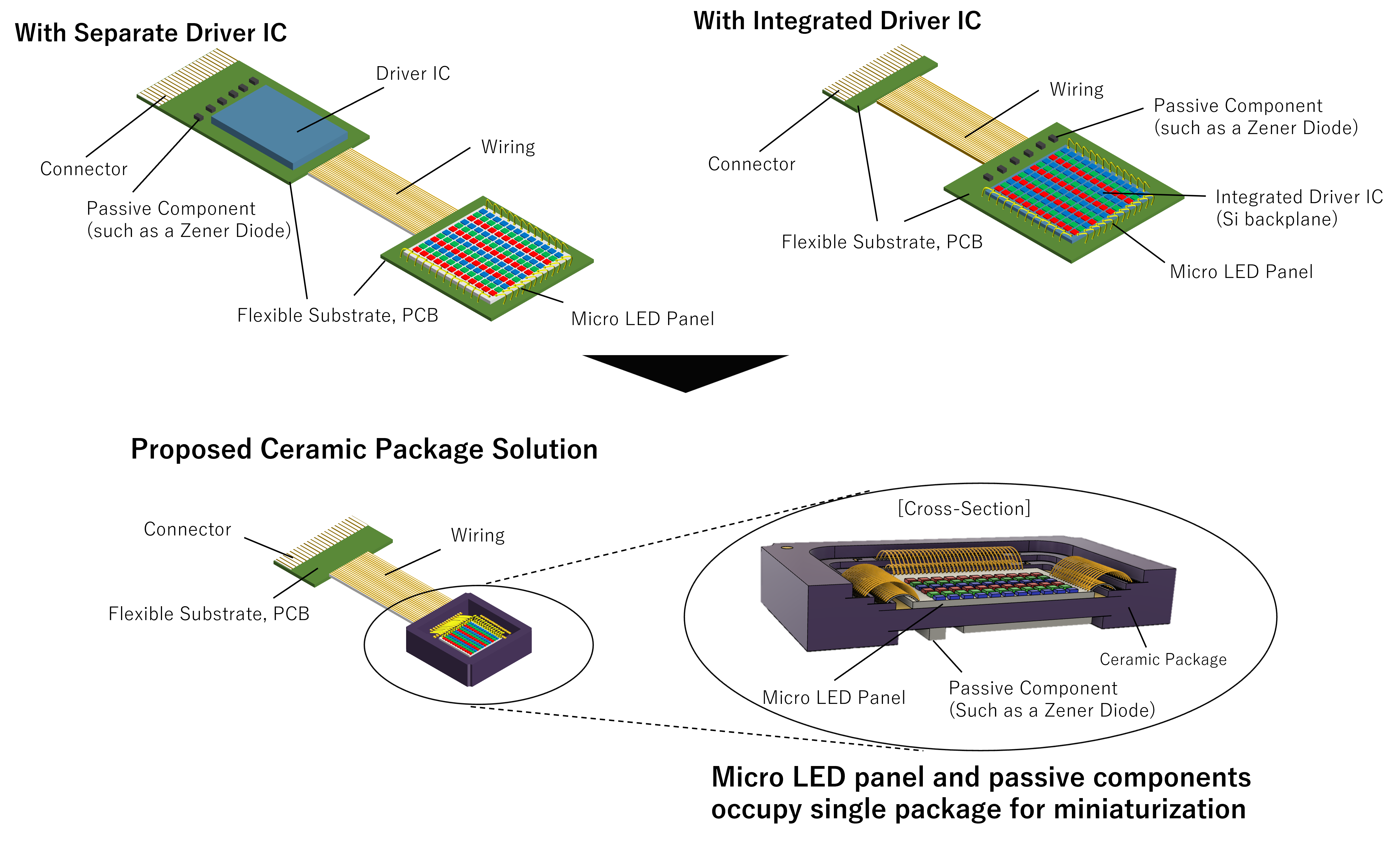
Ceramic packages can miniaturize Micro LED modules to make XR equipment more compact.
- Ceramic packages allow dual-cavity structures, greatly enhancing space efficiency and maximizing freedom of design.
- Further space saving is possible by packaging Micro LEDs in a ceramic package, which allows passive components (such as Zener diodes, resistors, etc.) to be integrated and mounted on the bottom side within one package.
Solution to Challenge #2
Thermal Management
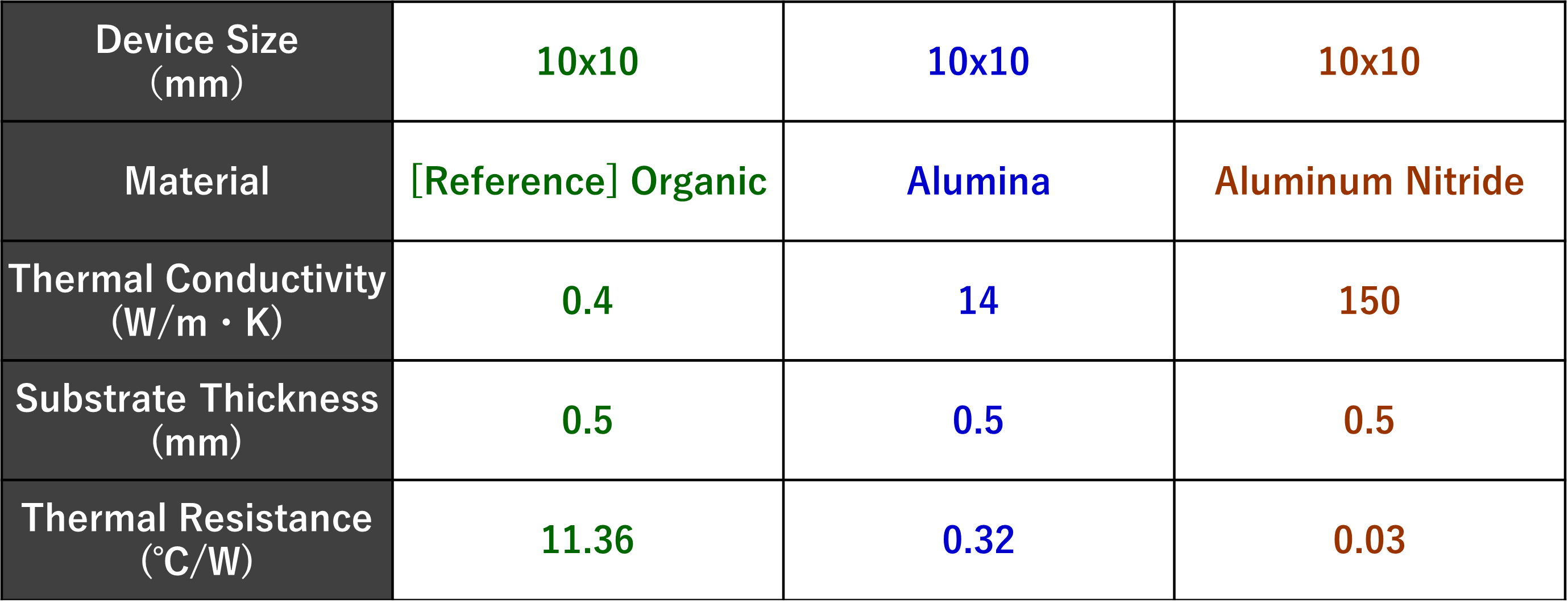
Ceramic packages dissipate heat efficiently, preventing malfunctions and heat-related device failures.
- Heat dissipation is enhanced by thermally conductive ceramics.
- The heat emitted by the Micro LED panel is efficiently dissipated by the ceramic package.
- Optimal materials can be selected, including alumina or aluminum nitride, based on the amount of heat generated.
Comparison: Thermal Conductivity by Package Material
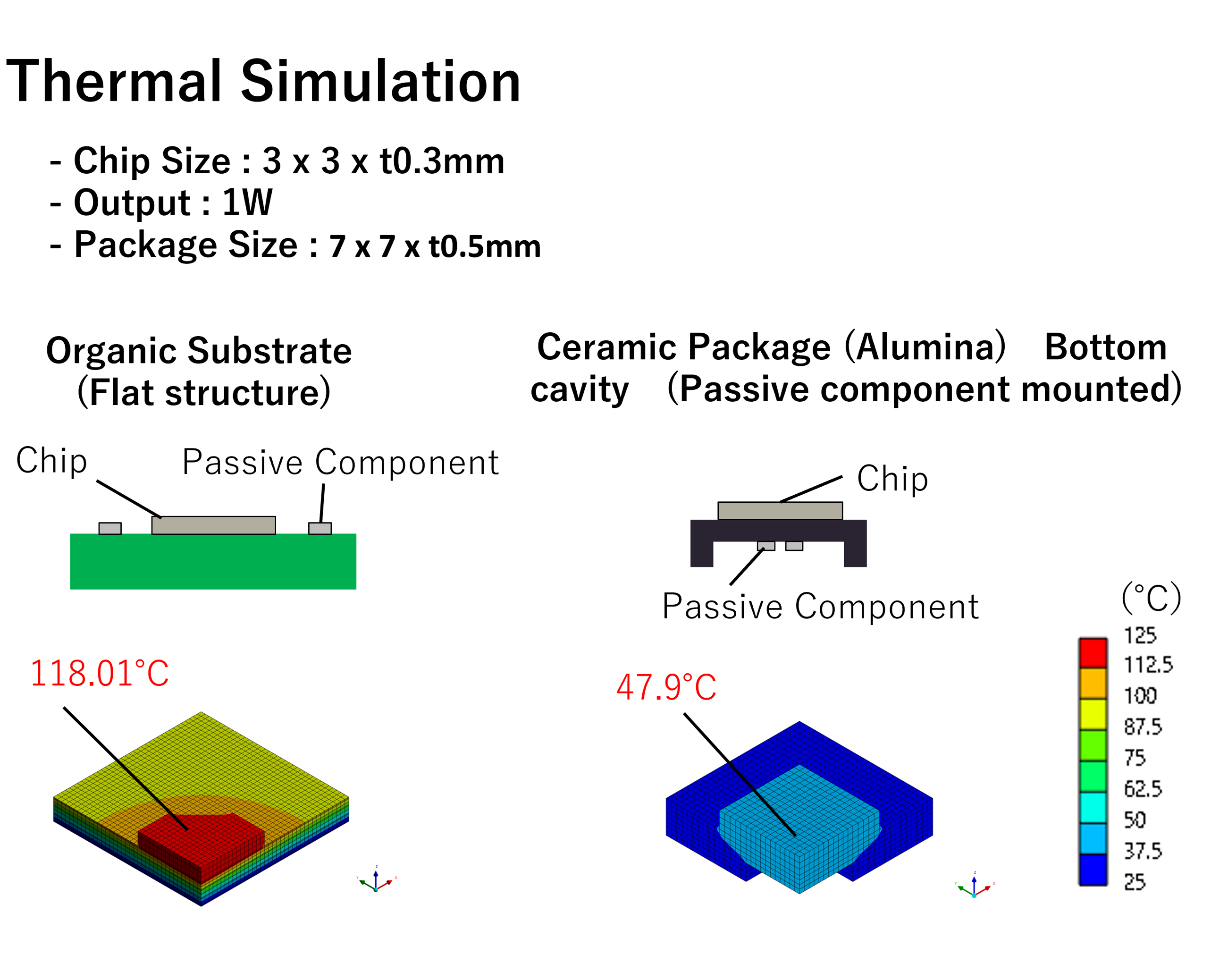
Challenge #1 (Miniaturization) + Challenge #2 (Thermal Management)
By combining the unique features of ceramic packages, Kyocera can create optimal solutions to your Micro LED challeges.
The simulation results on the left show how ceramic packages can enhance both module miniaturization and heat dissipation at the same time.
Higher heat dissipation is achieved even when passive components are mounted on the bottom side.
Solution to Challenge #3
Preventing Light Source Distortion
Ceramic packages greatly minimize substrate deformation and its effect on images.
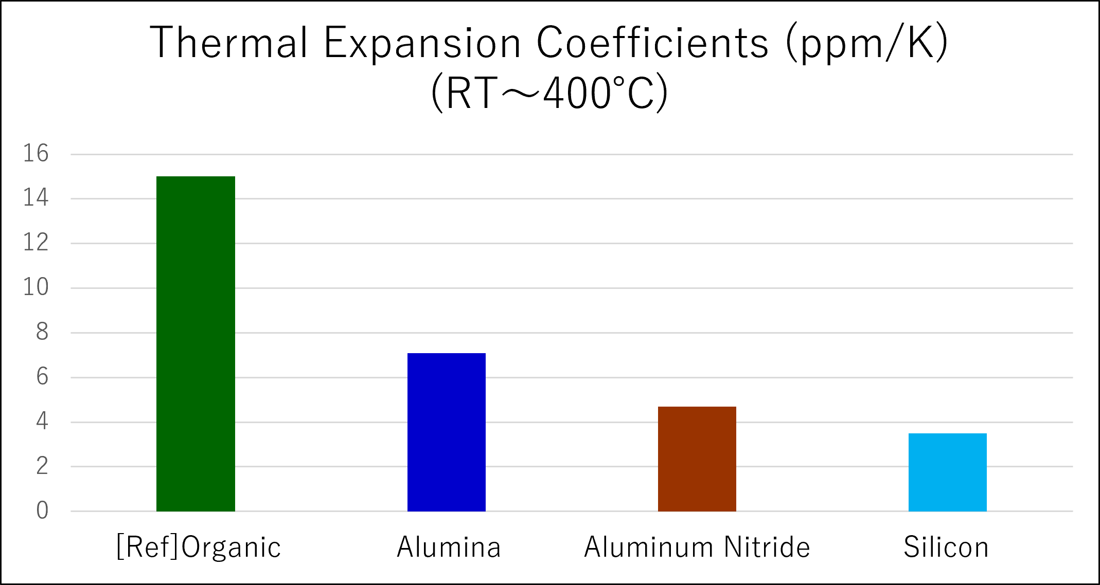
- The coefficient of thermal expansion (CTE) between the ceramic package and the silicon backplane can be closely matched (see figure 1).
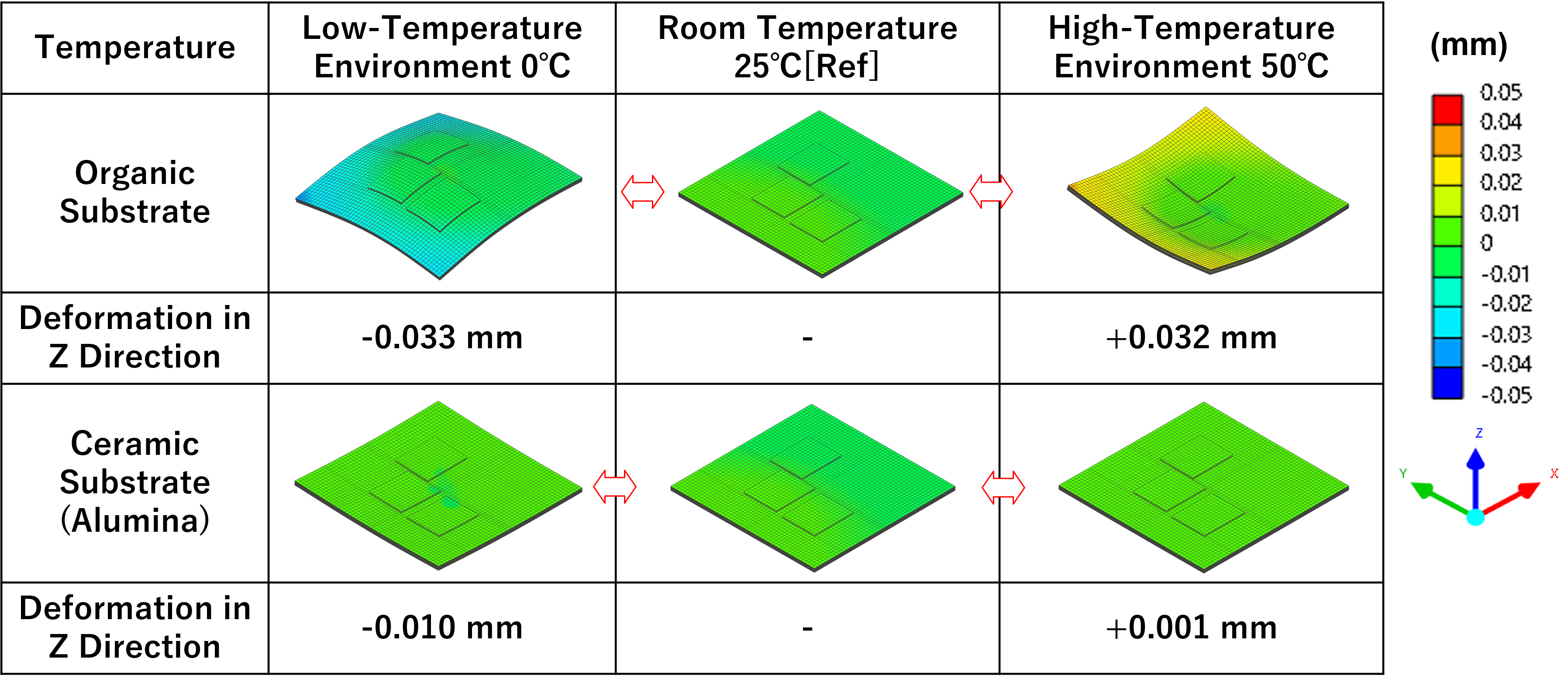
- Because ceramics are not easily deformed by temperature changes, substrate deformation is greatly reduced, along with the negative effects on image quality (see figure 2).
Comparison: Coefficients of Thermal Expansion
Simulation: Substrate Deformation and Temperature
Solution to Challenge #4
Providing Low-Loss, High-Density Wiring to Ensure Excellent Display Quality
The use of a ceramic package reduces transmission loss, relieving a key challenge associated with high pixel counts.
- The flexible design options available with ceramics can optimize electrical design and reduce electrical losses in Micro LED panels.
- Achieving low-inductance transmission lines results in a higher image quality.
Multilayer Design Increases Via Placement Freedom and Shortens Bonding Wires
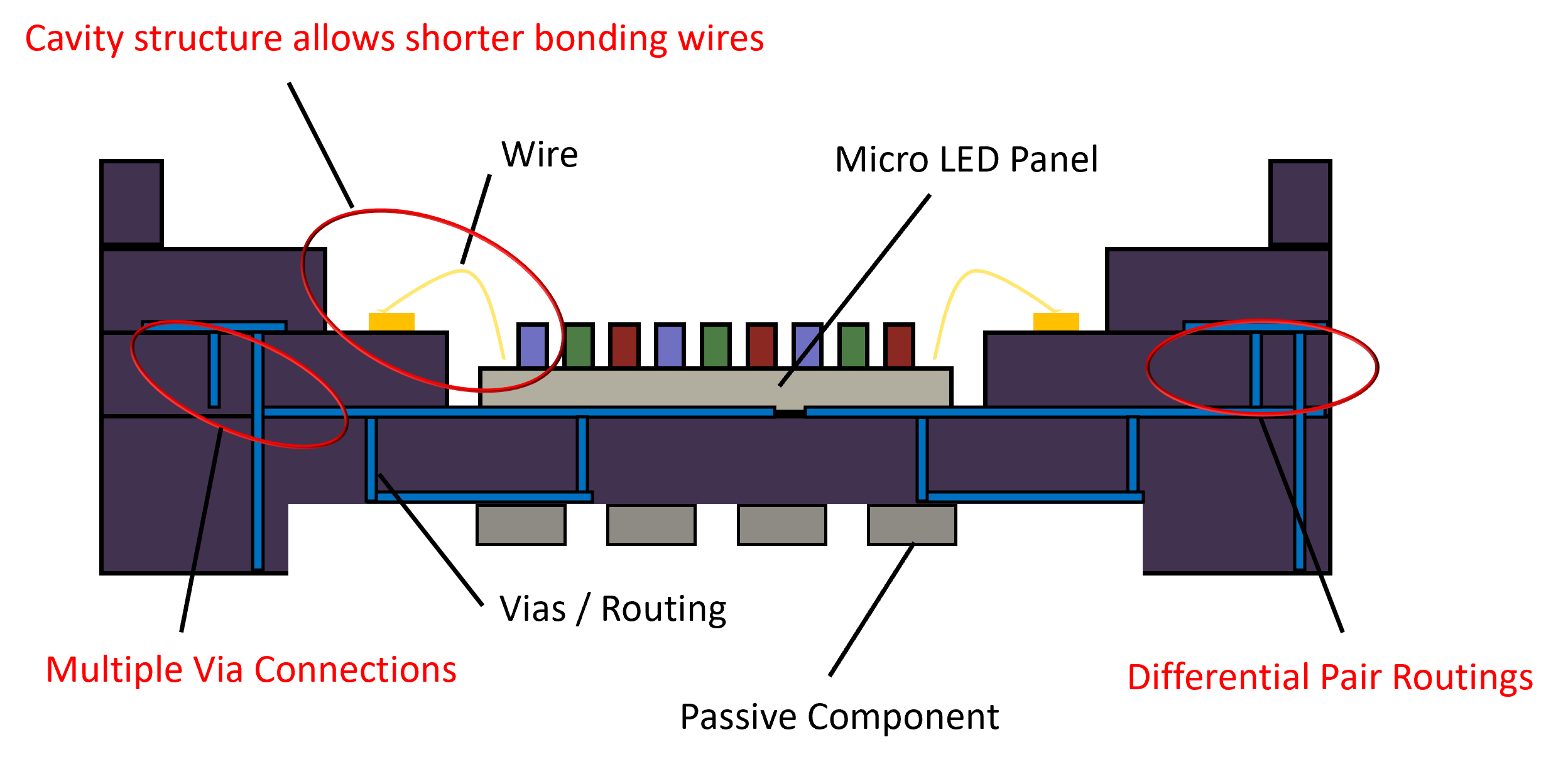
Multilayer routing simplifies via placement, allows shorter bonding wires, and contributes to lower inductance.
In addition, multilayer routing enables high-speed transmission for MIPI.
※MIPI:Mobile Industry Processor Interface
Advantages of Ceramic Packages
Ceramic package features and benefits
are also introduced on the following pages.
Click here for more information on the basics of
ceramic packaging technology.