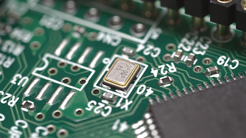
Electronic device performance continues to increase rapidly, driven by multifunctional smartphones, multi-device connectivity, high-speed infrastructure, connected vehicles, and the proliferation of IoT devices.
Achieving higher performance in devices of the same or smaller dimensions introduces new challenges, including increased heat generation due to higher-density mounting of semiconductors and electronic components; as well as increased heat output per device.
Efficient heat dissipation within a limited space has become a key factor in the development of electronic devices.
Among the ceramic materials used in components and packages, aluminum nitride is attracting broad attention across the electronics industry as a solution to this critical challenge. This page outlines the features of aluminum nitride, as well as the characteristics of aluminum nitride substrates and packages that Kyocera offers.
Features: What is Aluminum Nitride
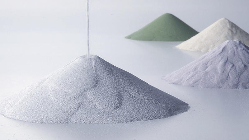
Aluminum Nitride (AlN) is a ceramic material synthesized from aluminum and nitrogen, known for its unique properties.
Its main features include:
-
Exceptionally High Thermal ConductivityAmong ceramic materials and metals, AlN offers exceptionally high thermal conductivity -- up to 10X higher than that of Alumina (Al2O3).
-
Electrical InsulationAlN exhibits excellent electrical insulation characteristics.
-
Lower Coefficient of Thermal Expansion (CTE)AlN's coefficient of thermal expansion is close to that of silicon (Si), the most common semiconductor material.
Consequently, when silicon chips are bonded to AlN, the CTE mismatch between substrate and chip is minimized, reducing risk of deformation and delamination.
Other features of AlN include high mechanical strength, excellent heat resistance, high chemical resistance, and low particle generation from the material surface.
Thanks to these properties, aluminum nitride is widely used in heat-dissipating substrates and packages for electronic components and devices. AlN is also commonly used in semiconductor manufacturing equipment, and as a filler in thermal interface and sealing materials.
Features of Kyocera's Aluminum Nitride Substrates / Packages
Kyocera offers aluminum nitride heat-dissipating substrates and packages for semiconductors and electronic components with the following features:
-
Material Properties
As introduced above, AlN has excellent material properties.
・High thermal conductivity (150 W/(m·K) or higher)
・High mechanical strength
・Coefficient of Thermal Expansion close to Si
・Low particle generation from material surface -
High Design Flexibility
Using a variety of processing technologies, Kyocera can manufacture substrates and packages tailored to custom requirements, including:
・Multilayer structure
・3D electrical interconnects between internal layers
・Thin-film processing on polished surface
・Metal plating/brazing technologies -
Hermetic Sealing Capability
AlN facilitates metallization to support hermetic sealing.
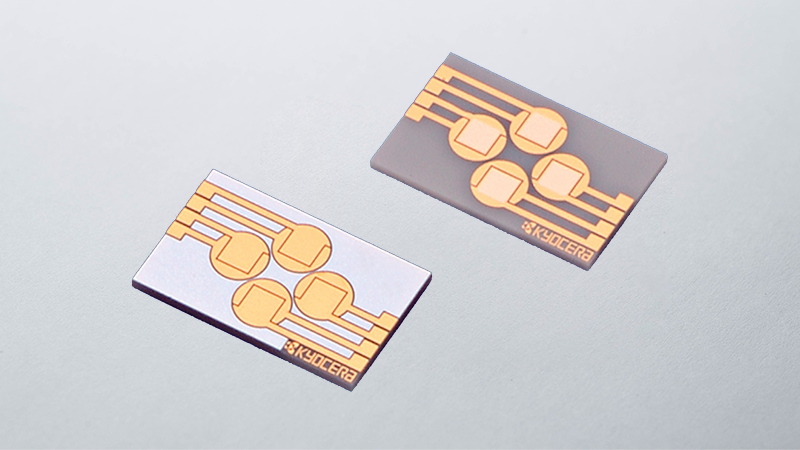
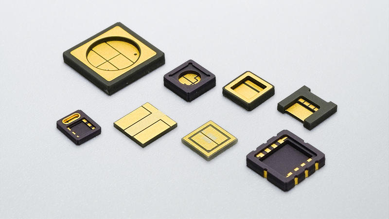
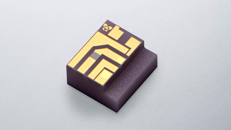
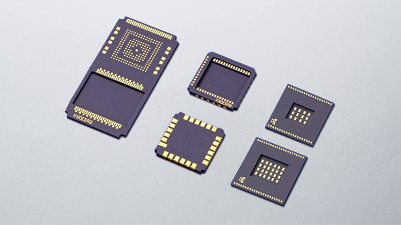
Case Study
Multilayer Structure
Below are examples of multilayer structures for aluminum nitride (AlN) substrates and packages.
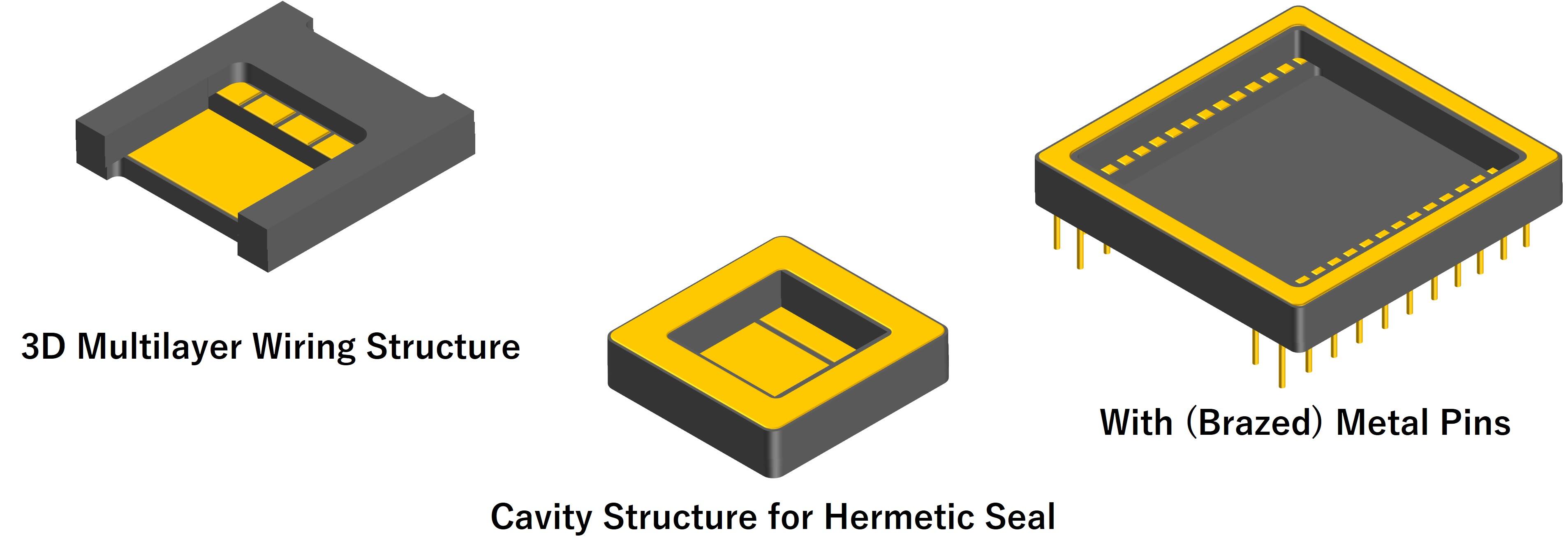
Kyocera can produce packages and substrates in a wide variety of designs, including customized multilayer structures, cavity configurations, and packages made by attaching metals (including pins) to ceramic.
Thin-Film Processing on Multilayer Substrates
Thin-film processing is also available for single-layer or multilayer AlN substrates.
Illustration below shows example of multilayer AlN substrate structure with thin-film metallization.
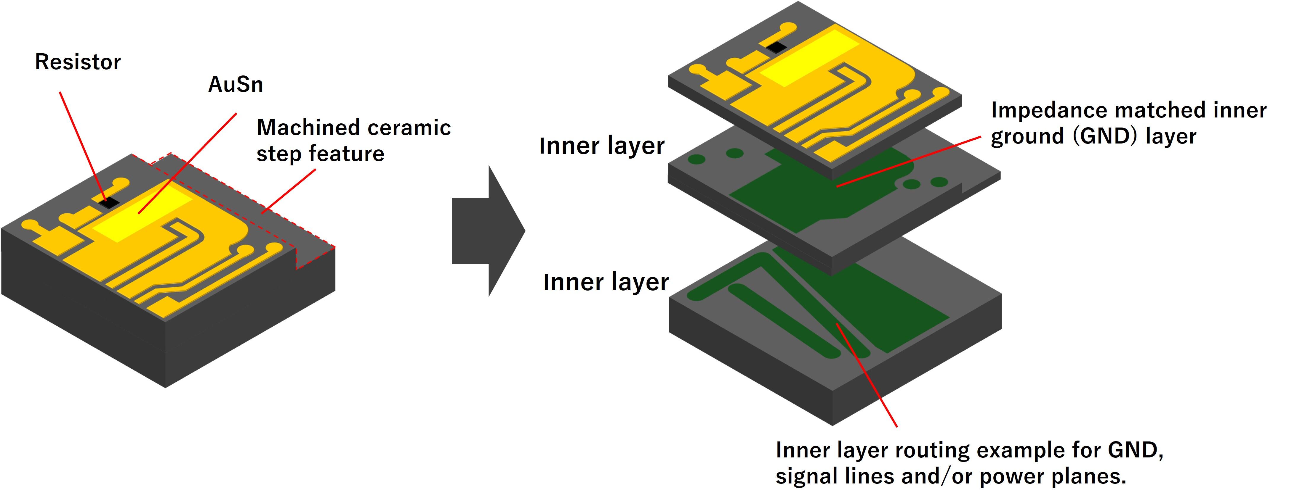
With a multilayer structure, wiring can be routed in the inner layers, enabling the formation of internal ground layers as well as impedance matching by separating signal routing from the ground layer.
In addition, thin-film technology can be applied to the surface layer to form circuit patterns, trimmable resistors, and AuSn pads. Additional machining processes can add mechanical features on any side of the package/substrate as well.
Material Properties

Applications
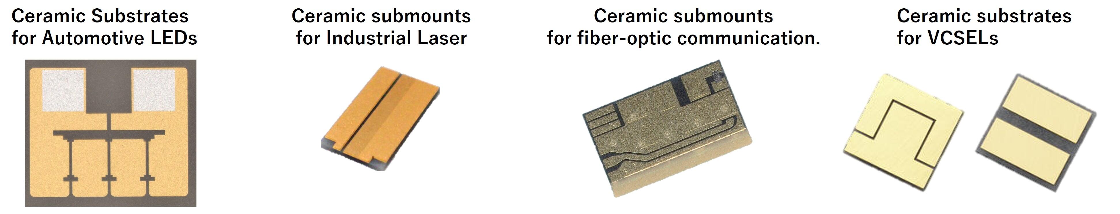
Specific Product Examples