
As part of our cultural activities, The Kyocera Museum of Fine Ceramics, located on the second floor of our global headquarters’ building in Kyoto, Japan, was opened to the public in October 1998. The museum showcases the evolution of Kyocera’s fine ceramic technology since the company’s founding in 1959. It is designed to provide a comprehensive understanding of fine ceramics, not only for students and researchers, but for visitors of all ages.
Global Headquarters Building and Museums
Basic Understanding of Fine Ceramics
Do you know the difference between ceramics and “fine ceramics?” The Museum begins with an introduction to fine ceramics, including the fundamentals of ceramic materials and processing technologies. An adjoining display shows the history of ceramics: from the earthenware of Japan’s Jomon Period (12,000-300 B.C.) through various pottery handed down throughout history, up to the emergence of today’s fine ceramics.
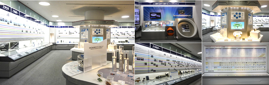
Kyocera’s Technology and Product Evolution
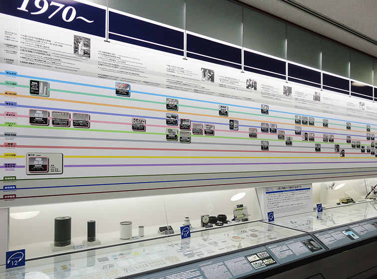
A wide variety of products developed by Kyocera are displayed chronologically from the company’s founding in 1959. This area explains the evolution of fine ceramic technology by showing actual Kyocera components; the end products that incorporate them; and a timeline of industrial and world events for historical context.
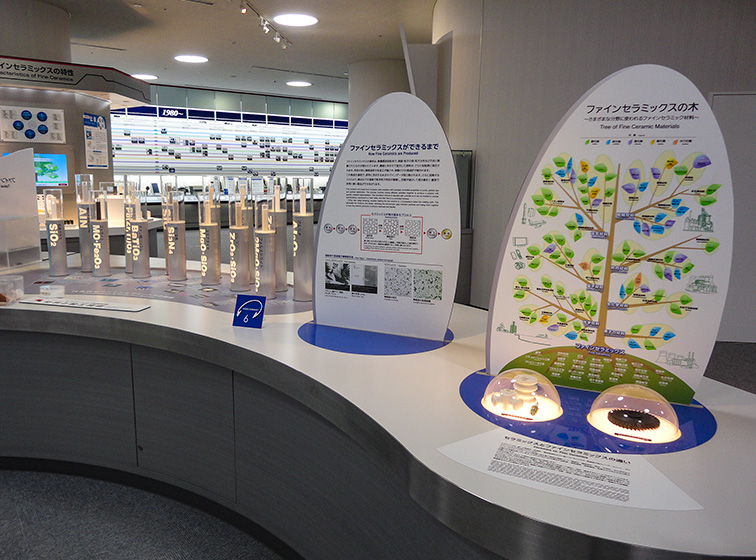
Characteristics of Fine Ceramics
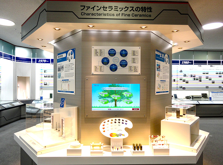
This area showcases the superior characteristics of fine ceramics including their high degree of hardness, rigidity, piezoelectricity and heat resistance. Video displays and hands-on demonstrations allow the visitor to gain a more thorough understanding of fine ceramics.
Fine Ceramics Help Expand the Boundaries of Scientific Research
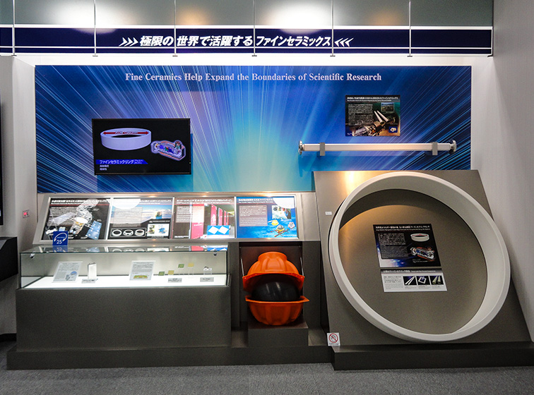
Here visitors can see real world examples of fine ceramics which are being utilized in cutting-edge scientific research projects: from battery terminals that protect lithium-ion batteries used in the “Hayabusa” space probe, to pressure-resistant containers for seismometers which are employed at a depth of 11,000 meters in the ocean.
History of Ceramic Packages in the Semiconductor Industry
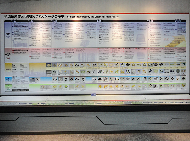
A large display panel stretching 5 meters in width shows the history and evolution of Kyocera’s ceramic packages which have continually supported the development of the semiconductor industry.