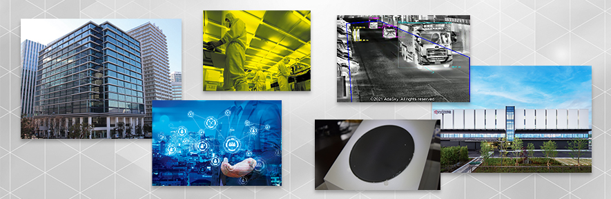
Creating New Value for Society with Open Innovation and Collaboration
The Kyocera Group promotes open innovation, collaboration, and M&A activities across our global network.
We aim to be pioneers who create new value at the cutting edge of technology.
Addressing Social Needs with Cutting-Edge Technology
Cooperative Road-Vehicle System
Kyocera’s Cooperative Road-Vehicle System enables communication and cooperation between vehicles equipped with driving automation features, other road users, and transportation infrastructure, to enhance safety and manage roadway congestion. It communicates essential data using ITS wireless roadside units to warn drivers of danger. Successful development of this system will help commercialize autonomous driving, which cannot be achieved through smarter vehicles alone. The Cooperative Road-Vehicle System represents a key technology that will enable next-generation transportation, improving safety and security for everyone on the road.
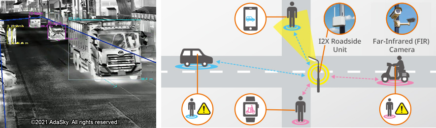
Detection screen (left) and the Cooperative Road-Vehicle System concept diagram (right)
Micro-LED / Proprietary Micro-Laser Substrate
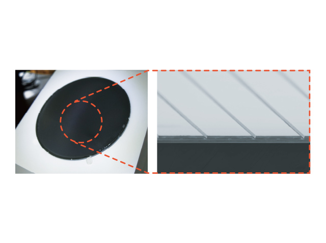
Our proprietary technology allows us to create three-dimensional structures in multilayer substrates using ultra-low-defect GaN*1 and other materials, including low-cost silicon or sapphire, yielding proprietary EGOS*2 substrates. Using this technology, micro-light sources*3, such as micro-LEDs, can be manufactured in high volumes on a substrate and stripped off at a low defect rate and low cost. Micro-light sources are expected to be used in applications ranging from automotive displays to next-generation smart glasses.
*1 GaN: Gallium nitride*2 EGOS: Epitaxial lateral overgrowth GaN On Substrate.
*3 Micro-light source: A light source with one side of an element less than 100 micrometers (μm).
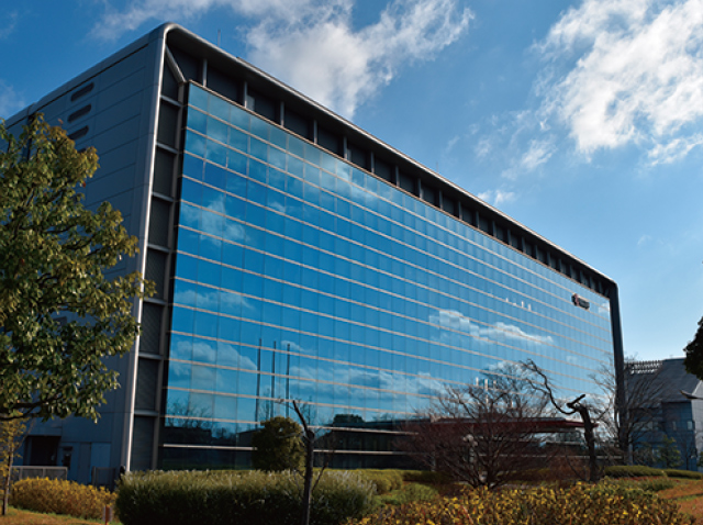
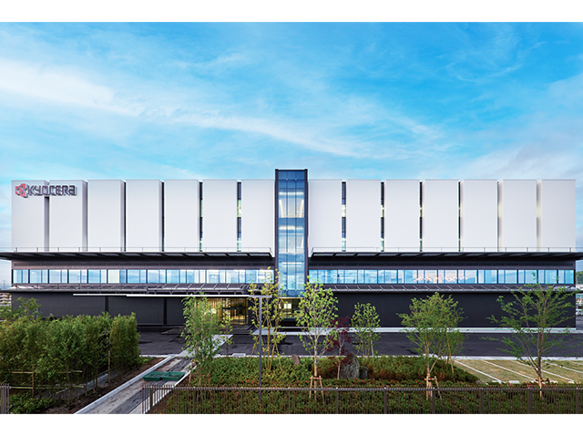
Main R&D Facilities
Kyocera operates a global R&D network to deepen our technological capabilities in materials, components, devices, equipment, systems, software, and production process technology.
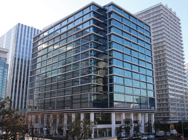
Minatomirai Research Center
(Yokohama, Japan)
Keihanna Research Center
(Kyoto, Japan)
Kirishima R&D Center
(Kagoshima, Japan)
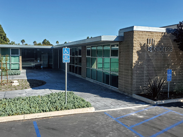
Santa Barbara Innovation Center
at KYOCERA SLD Laser, Inc.
(California, U.S.A.)
*Develops GaN devices