Device Mounting Methods
There are two main methods for mounting IC chips onto ceramic packages: wire bonding and flip-chip. Ceramic packages support either method.
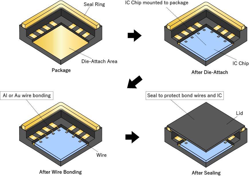
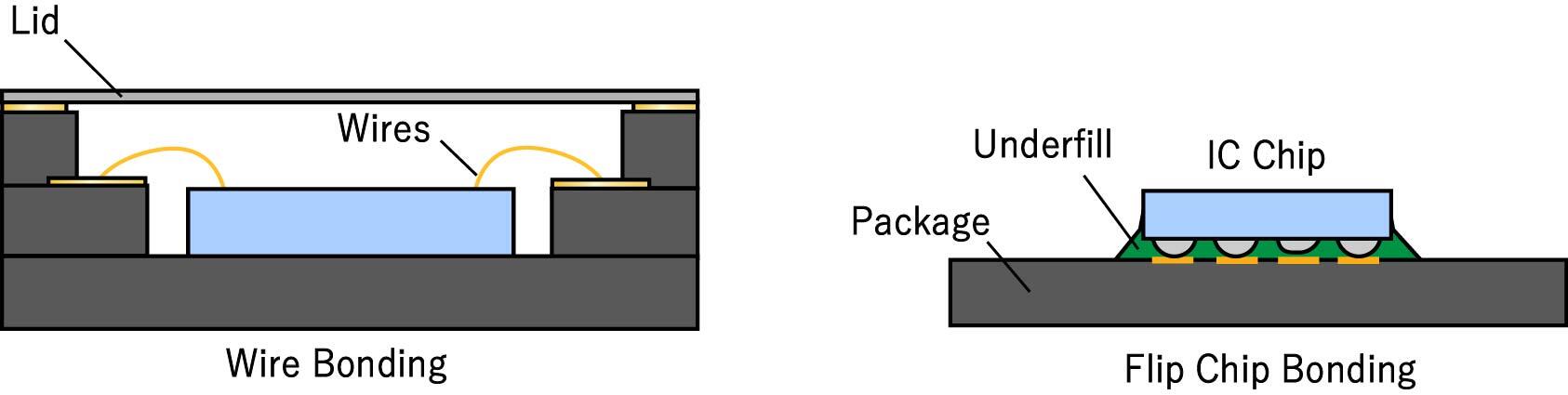
Wire Bonding
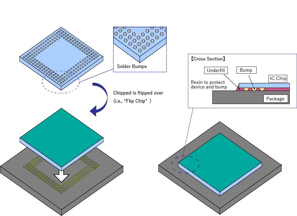
Flip Chip Bonding
Ceramic Packages: Wire Bonding or Flip Chip Bonding
Ceramic packages are manufactured by laminating multiple layers, one by one, making it easy to form 3-D structures, including space-saving 3-D circuit patterns. In wire-bond packages, a ceramic bonding shelf can shorten bonding wires for improved electrical characteristics. Ceramic offers key advantages for flip-chip bonding as well. With coefficients of thermal expansion (CTE) closer to that of silicon, ceramic materials improve reliability by minimizing expansion mismatch during assembly and operation. Kyocera also offers ceramic materials with CTE closer to that of organic printed circuit boards, improving board-level reliability by reducing thermal stress in field operations.