Redefining performance in large HDBU (High-Density Build-Up) packaging, multilayer ceramic core substrates provide unmatched rigidity and thermal stability, maintaining structural integrity where conventional organic materials fall short

Rising performance and complexity in advanced semiconductors is creating demand for new HDBU packaging technologies that integrate multiple IC chips (chiplets) onto silicon interposers. Further gains in performance require interposers, and package substrates in larger dimensions, introducing new challenges with warping, thermal stress, and cracking. Kyocera is developing multilayer ceramic core substrates with high rigidity and high strength to overcome these challenges in HDBU packaging.
Outline
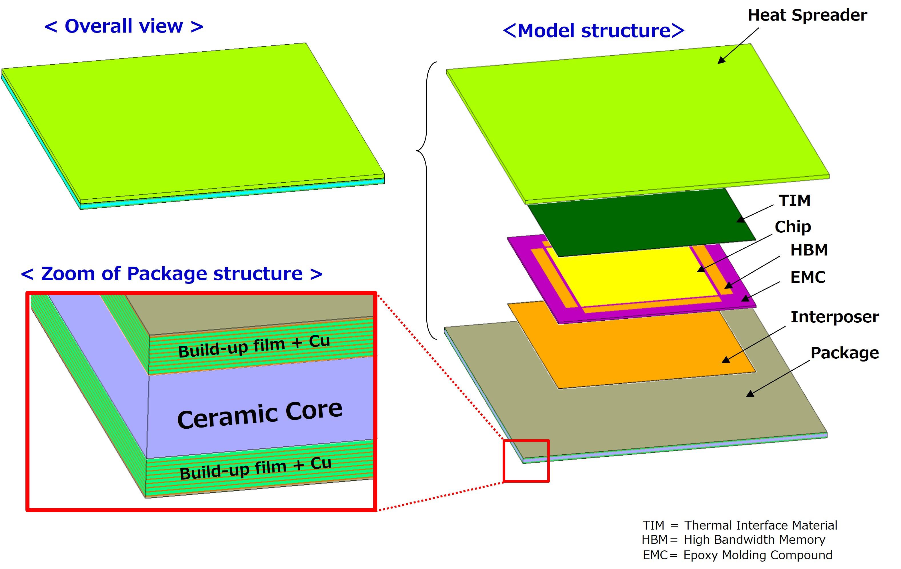
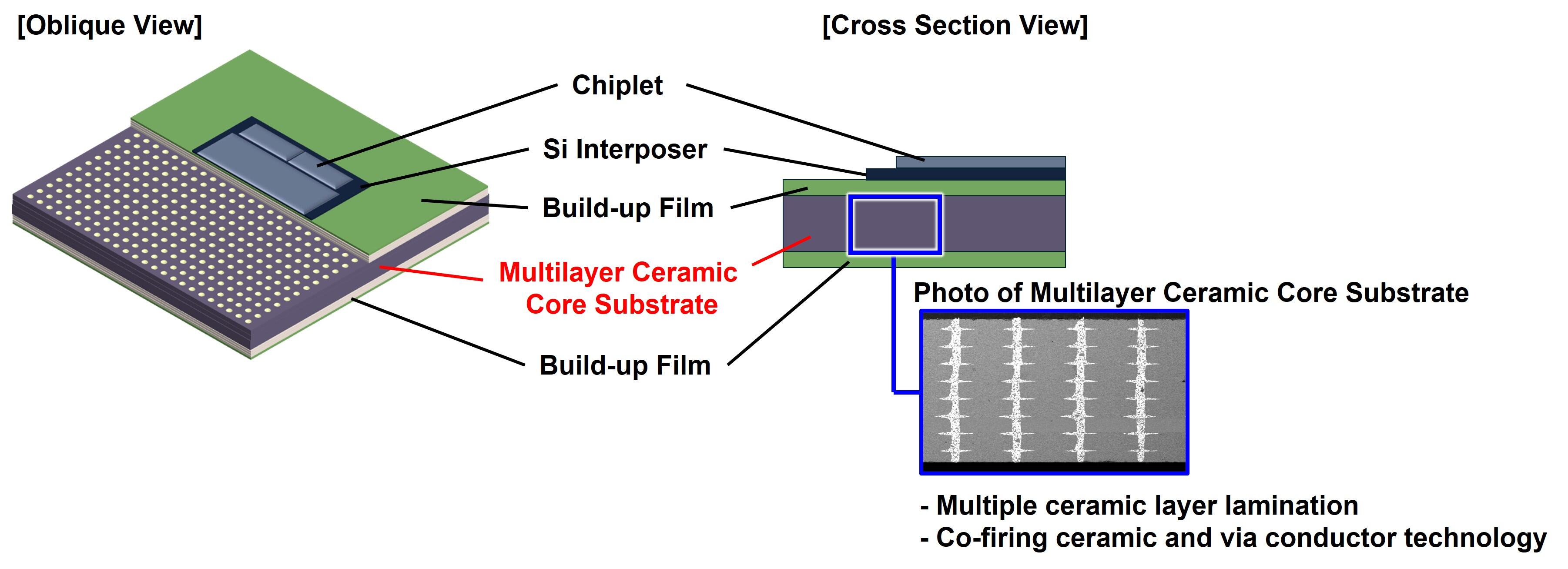
Multilayer ceramic core substrate
Kyocera supplies only multilayer ceramic core substrates.
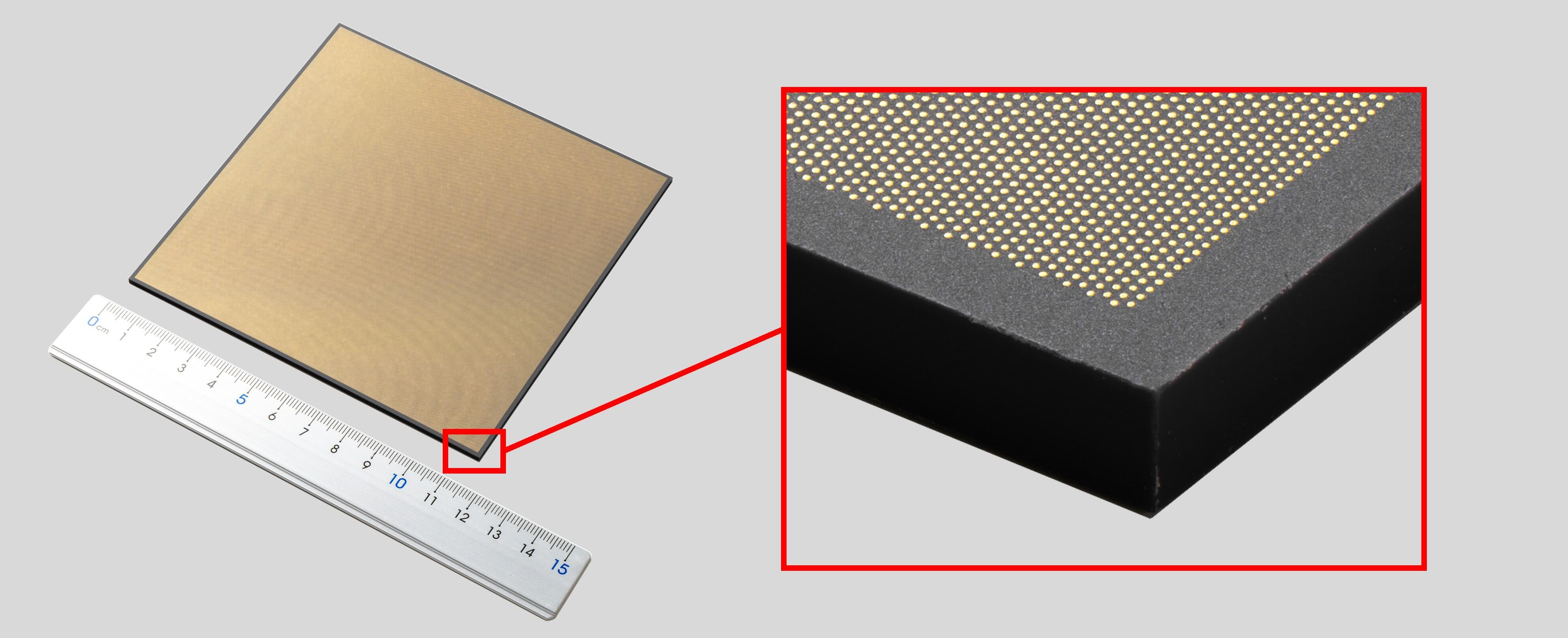
Typical Size and Expanded View
Features


High Young's modulus (rigidity) to suppress substrate warpage and high mechanical strength to withstand thermal stress
Large package substrates for advanced semiconductors are manufactured by laminating a build-up film onto a core substrate. Unless the core material exhibits high Young's Modulus, stresses generated during the build-up film lamination and chiplet mounting processes can cause substrate warpage. In addition, the core substrate must exhibit high mechanical strength to prevent cracking under thermal stress during the assembly process. Organic core materials, widely used for general-purpose large-package substrates, experience warpage after chiplet mounting due to the organic material’s lack of rigidity. Glass core materials, which are being studied as an alternative, encounter "Seware(*)". Kyocera is developing multilayer ceramic core materials with high rigidity and high strength to solve these issues.
(*) Seware : A mode of destruction caused by insufficient strength of a core substrate against stresses during build-up film lamination or IC chip mounting
The following simulation results compare post-assembly warpage in organic, glass, and ceramic core materials. Ceramic materials show the least warpage.
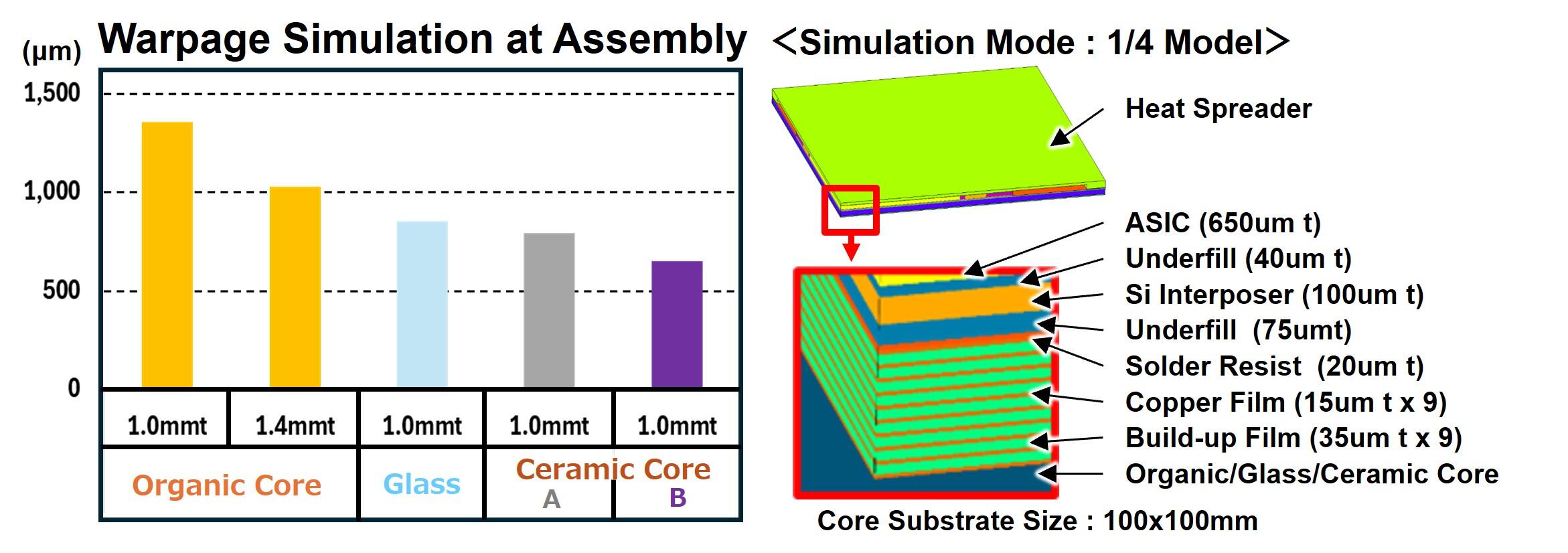
Material properties

Simulation support
Kyocera can support virtually any design using our world-class simulation tools, which include stress simulation, electrical simulation, thermal simulation and others, according to customer requirements.
Click below for Details.