
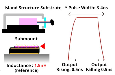
Kyocera’s ceramic packages provide outstanding heat dissipation and heat resistance properties, contributing to reduced inductance for the entire LIDAR module.
Lower inductance packaging enables high power and narrow pulse width lasers.
-
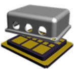
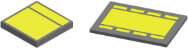
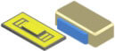
Side-Windowed
Package -
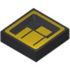
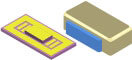
Island Package
and Side-Windowed Lid -
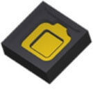
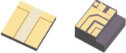
Edge-Emitting
Laser Package -
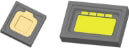
VCSEL
Package
Kyocera’s Pulse LiDAR Package Solutions
Package Technology for Long Distance Detection
- Technical Requirements for Long Distance Detection
-
- Increased Pulse Frequency
- Additional Laser Power
- Eye Safe Laser
- Technical Challenges
-
- Low Inductance requirements
- Improved heat dissipation from laser
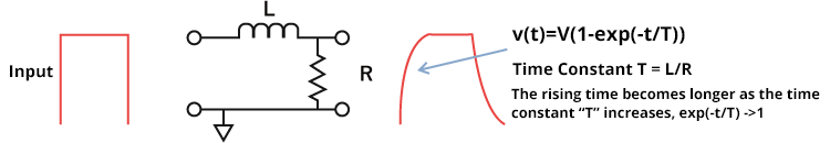
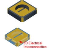
Low Inductance Packaging
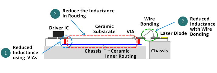
Multilayer ceramic packaging can reduce inductance using a VIA structure design that results in shortened wire bond lengths.
(1) Optimization of VIA count
(2) Minimizing wire bond loop length with a cavity structure
(3) Parallel routing in two layers (patent pending)
-
1Allocate Multiple VIAs(◿67%) 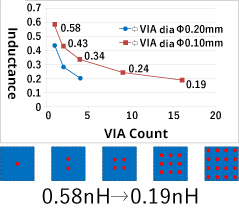
Reduces inductance by allocating more VIAs in multilayer ceramics.
-
2Minimizing Wire Length(◿54%) 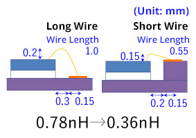
Reduces inductance by adding bonding shelf to minimize wire bond length.
-
3Parallel Routing in Ceramics Connection through VIAs(◿31%) 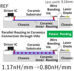
Reduces inductance by parallel routing within two ceramic layers and connection of VIAs
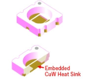
Improved Heat Dissipation from Laser
Adopting a high thermal conductive ceramic material provides improved heat dissipation from the device and suppresses the temperature rise, allowing for optimal laser diode performance.
Additional heat dissipation is required from the package to compensate for the integration of multiple functionalities. The benefit of using ceramic packaging and materials is the ability to integrate multiple components, such as multi-laser chips, photodiodes, steering devices, and Control ICs.
High Thermal Conductivity Ceramic Materials Line-up
◎: Excellent ○: Good △: Okay
| Multilayer Alumina |
Multilayer Aluminum Nitride |
CuW Embedded Multilayer Alumina |
||
|---|---|---|---|---|
| Kyocera Material Code | A473 | AN242 | AO610W | |
| Structure Design |
 |
 |
 |
|
| Thermal Conductivity (W/mK) | △ 18 | ◎ 150 |
○ Alumina:17
CuW:200 |
|
| Coefficient of Thermal Expansion (/K) | ○ 6.9×10⁻⁶ | ◎ 4.7×10⁻⁶ | ○ 6.8×10⁻⁶ | |
| Chip Connection | Wire Bonding | ◎ | ◎ | ◎ |
| Flip Chip | ◎ | ○ | △ | |
| Miniaturization | ◎ | ○ | △ | |
| Cost Comparison for 3 Materials※ | Low | High | Middle | |
Comparison between A473, AN242 and AO610W.
High Thermal Conductivity Ceramic Materials Line-up
| Multilayer Alumina | ||
|---|---|---|
| Kyocera Material Code | A473 | |
| Structure Design |
|
|
| Thermal Conductivity (W/mK) | △ 18 | |
| Coefficient of Thermal Expansion (/K) | ○ 6.9×10⁻⁶ | |
| Chip Connection | Wire Bonding | ◎ |
| Flip Chip | ◎ | |
| Miniaturization | ◎ | |
| Cost Comparison for 3 Materials※ | 低 | |
| Multilayer Aluminum Nitride | ||
|---|---|---|
| Kyocera Material Code | AN242 | |
| Structure Design |
|
|
| Thermal Conductivity (W/mK) | ◎ 150 | |
| Coefficient of Thermal Expansion (/K) | ◎ 4.7×10⁻⁶ | |
| Chip Connection | Wire Bonding | ◎ |
| Flip Chip | ○ | |
| Miniaturization | ○ | |
| Cost Comparison for 3 Materials※ | High | |
| CuW Embedded Multilayer Alumina | ||
|---|---|---|
| Kyocera Material Code | AO610W | |
| Structure Design |
|
|
| Thermal Conductivity (W/mK) |
○Alumina:17
CuW:200 |
|
| Coefficient of Thermal Expansion (/K) | ○ 6.8×10⁻⁶ | |
| Chip Connection | Wire Bonding | ◎ |
| Flip Chip | △ | |
| Miniaturization | △ | |
| Cost Comparison for 3 Materials※ | Middle | |
Comparison between A473, AN242 and AO610W.
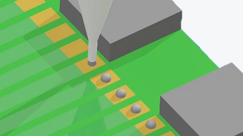
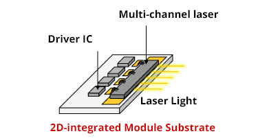
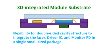
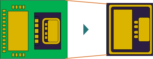
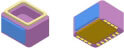
Single and Double-sided Mounting for Miniaturization and Cost Reduction
2D and 3D modules are required to achieve high performance, miniaturization, and lower cost. Therefore, the Laser, Driver IC, and Monitor PD are integrated into a single small-sized module.
Solutions
Kyocera has developed a unique forming and lamination process for manufacturing double-cavity structure packages in large volumes.
Integrating the laser, driver IC, monitor PD, and chip caps to 2D and 3D modules enable miniaturization and cost reduction.
In addition, this integration of devices provides the added benefit of reducing inductance with shorter routing lengths by having routing inside package.
Kyocera’s cavity and double-sided cavity packages provide improved module size and long-term performance.
- CASE
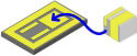
1Edge-Emitting Laser (EEL) + Driver IC -
Driver IC (Wire Bonded)
Side-Windowed Wire Bonding Package
Module Area: 8.40 x 7.00mm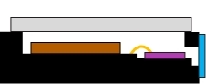
Driver IC (Flip Chip Bonding)
Side-Windowed Solder Pad Package
Module Area: 6.10 x 6.60mmReduces module size by 32% and eliminates wire bonds between the Driver IC and the laser, contributing to reduced electrical inductance.
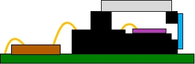
- CASE
2VCSEL + Driver IC -
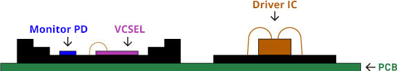
1.2D-Module (on Flat Substrate) 
2.2D-Module (on Cavity Package) 
3.3D-Module 
- Chip Size (Estimation)
-
- Monitor PD :1×1mm
- VCSEL:5×4mm
- Driver IC :3×6mm
1. and 2. : Reduced Module Size by 25%,
3. : Reduced Module Size by 40%.
Eliminates wire bonds between the Driver IC, EEL and VCSEL to enable reduced inductance.
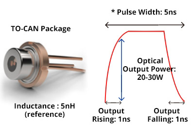
Comparison of TO-CAN and Ceramic Package
When comparing the thermal resistance of TO-CAN packages and ceramic packages with AlN (Aluminum Nitride), there is no change in the package’s thermal resistance, even with a significant size reduction. The maximum heat resistance of the package is approximately 50% lower than a TO-CAN package of the same size.
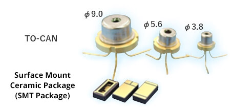
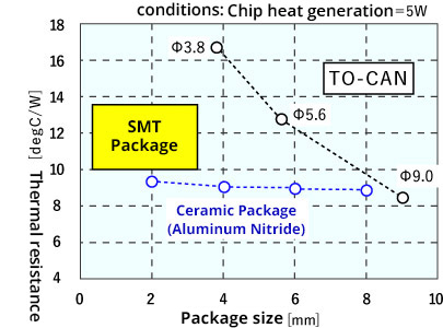
Benefits of Leadless Packaging and Ceramic Substrate Materials
Ceramic leadless packages provide higher thermal conductivity and allow the thermal path to be routed through the backside of the package. This enables better heat dissipation than a traditional TO-CAN Package.
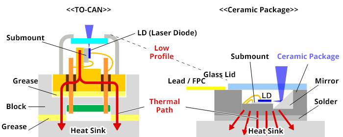
Surface mount ceramic package designs offer a lower profile module with a more effective thermal path than TO-CAN packages.
Additionally, ceramic packages reduce inductance by routing through multilayer ceramics. Therefore, the inductance of ceramic packages is about 50% lower than TO-CAN packages. (Example: Driver IC integrated module)
Inductance Simulation of Driver IC and Laser Diode
| Package Configuration | TO-CAN | Ceramic Package |
|---|---|---|
| Structure |
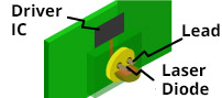 |
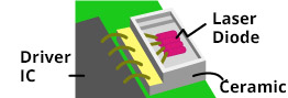 |
| Wiring / Routing Length (Driver IC – Laser Diode) (mm) | 7.65 | 3.88 |
| Inductance (nH) | 4.24 | 1.94 |
Ceramic Package Line-up
Kyocera develops a wide range of ceramic packages for nearly any type of laser.
Below is a list of Kyocera’s ceramic package offerings for different laser types
| Laser Type | Structure | Thermal Dissipation |
Substrate and Package Configuration |
|---|---|---|---|
| VCSEL | Submount | Moderate |
|
| High |
|
||
| Cavity Package |
Moderate |

|
|
| High |
|
||
| Edge-Emitting LD (EEL) |
Submount | Moderate |

|
| High |
|
||
| Cavity Package |
Moderate |
|
|
| High |
|


Lineup of ceramic packages by emmit direction
◎: Excellent ○: Good △: Okay
| Emitting Direction | Laser Type | Configuration | Structure | X-Section | Features | Heat Dissipation | Narrow Pulse | Reliability | Low Profile Miniaturization |
Package Cost |
|---|---|---|---|---|---|---|---|---|---|---|
| Horizontal | Edge- Emitting LD (EEL) | Island |
 |
 |
Submount Eliminated Lower Cost (Alumina) Hermetic Package Available |
○ | ◎ | ◎ | ◎ | ◎ |
| Side Window |
 |
 |
Submount Eliminated Hermetic Package Available |
○ | ◎ | ◎ | ◎ | ○ | ||
| Couch |
 |
 |
High Thermal Dissipation (AlN) Submount Eliminated |
◎ | ◎ | ◎ | ◎ | △ | ||
| Substrate |
 |
 |
High Thermal Dissipation (AlN) / Good Flatness / Fine Design / AuSn Pre-solder |
◎ | ○ | ◎ | ◎ | ○ | ||
| Vertical | Edge-Emitting LD (EEL) | CAN |
 |
 |
AlN pre-attached TO CAN Package | ○ | ○ | ◎ | △ | △ |
| Cavity |
 |
 |
High Thermal Dissipation (AlN) Hermetic Package Available |
◎ | ◎ | ◎ | ◎ | △ | ||
| VCSEL | Cavity |
 |
 |
High Thermal Dissipation (AlN) Hermetic Package Available |
◎ | ◎ | ◎ | ◎ | △ | |
| Substrate |
 |
 |
High Thermal Dissipation (AlN) / Good Flatness / Fine Design / AuSn Pre-solder |
◎ | ○ | ◎ | ◎ | ○ |
Lineup of ceramic packages by emmit direction
| Emitting Direction | Horizontal | |||
|---|---|---|---|---|
| Laser Type | EEL | |||
| Configuration | Island | Side Window | Couch | Substrate |
| Structure |
|
|
|
|
| X-Section |
|
|
|
|
| Features | Submount Eliminated Lower Cost (Alumina) Hermetic Package Available |
Submount Eliminated Hermetic Package Available |
High Thermal Dissipation (AlN) Submount Eliminated |
High Thermal Dissipation (AlN) / Good Flatness / Fine Design / AuSn Pre-solder |
| Heat Dissipation | ○ | ○ | ◎ | ◎ |
| Narrow Pulse | ◎ | ◎ | ◎ | ○ |
| Reliability | ◎ | ◎ | ◎ | ◎ |
| Low Profile Miniaturization | ◎ | ◎ | ◎ | ◎ |
| Package Cost | ◎ | ○ | ○ | ○ |
| Emitting Direction | Vertical | |||
|---|---|---|---|---|
| Laser Type | EEL | VCSEL | ||
| Configuration | CAN | Cavity | Cavity | Substrate |
| Structure |
|
|
|
|
| X-Section |
|
|
|
|
| Features | AlN pe-attached TO CAN Package | High Thermal Dissipation (AlN) Hermetic Package Available | High Thermal Dissipation (AlN) Hermetic Package Available | High Thermal Dissipation (AlN) / Good Flatness / Fine Design / AuSn Pre-solder |
| Heat Dissipation | ○ | ◎ | ◎ | ◎ |
| Narrow Pulse | ○ | ◎ | ◎ | ○ |
| Reliability | ◎ | ◎ | ◎ | ◎ |
| Low Profile Miniaturization | × | ◎ | ◎ | ◎ |
| Package Cost | × | ○ | ○ | ○ |