Chip-Level Assembly Options
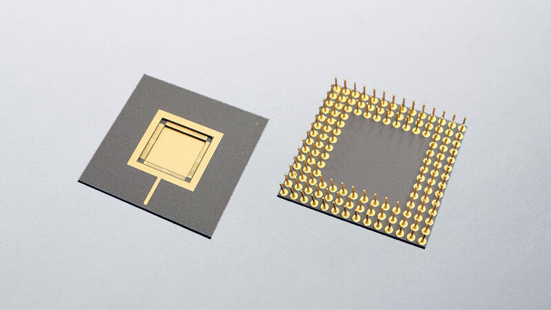
The process of mounting an IC chip onto a package is known as "chip-level assembly" (see options below). Since ceramic packages are manufactured through a process of laminating multiple layers, each with its own circuit patterning, three-dimensional circuitry within the package itself is easy to design and produce.
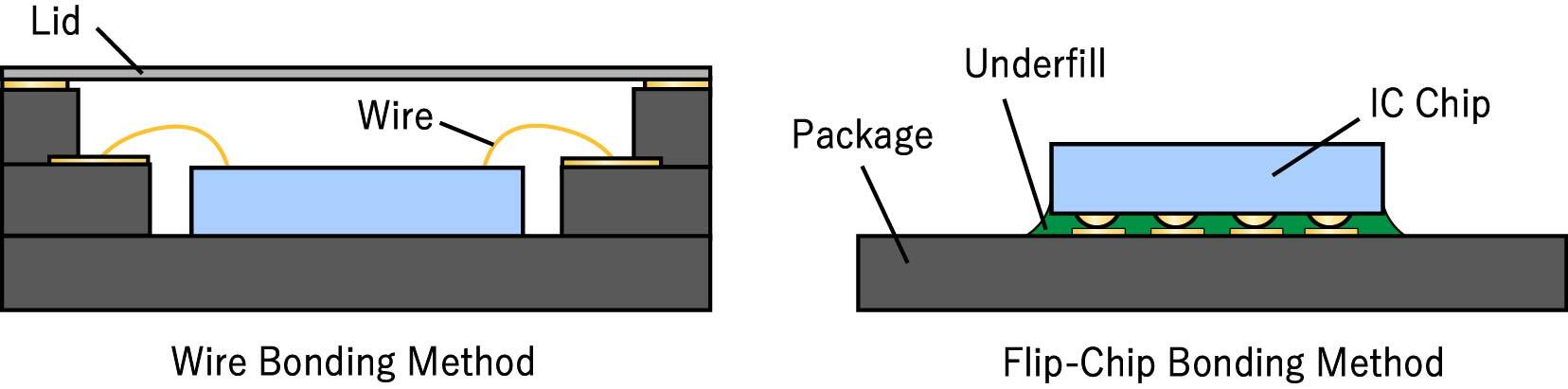
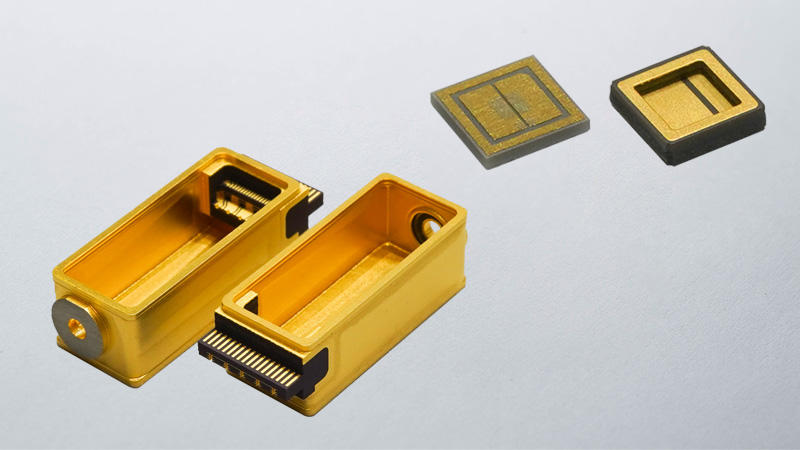
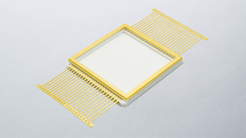
Wire bonding: Ceramic packages allow the formation of a bonding shelf, which enables shorter bonding wires for improved electrical characteristics.
In addition, the box-shaped cavity structure simplifies sealing.
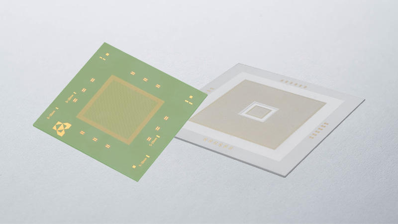
Flip-chip bonding: Ceramics with coefficients of thermal expansion closer to that of the IC chip itself (typically silicon) improve device reliability by minimizing thermal stress during assembly.
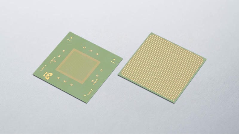
Board-Level Assembly Options
Mounting a packaged IC device on a printed circuit board and making its electrical connections is known as "board-level assembly".
Board-level assembly applies to a wide variety of assembly methods and package types.
Kyocera offers advanced manufacturing processes to create high-precision multilayer ceramic structures, as well as technologies to bond ceramics to metals, which expand the range of board-level assembly options.
We can deliver either standard package solutions for board-level assembly or customized package designs for your specific needs.
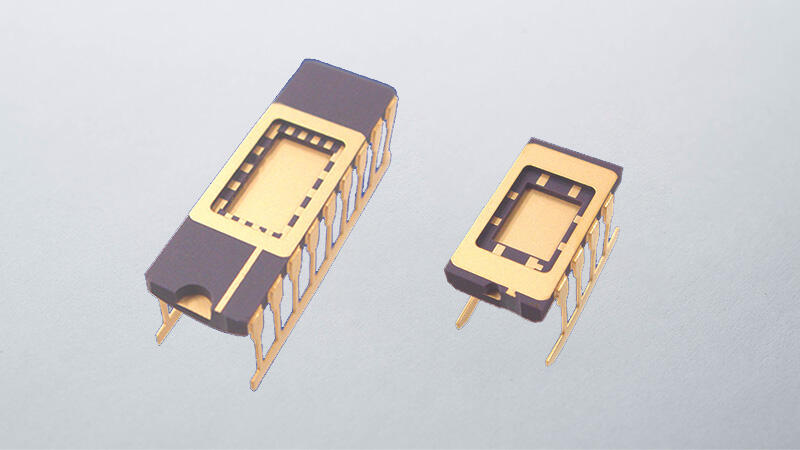
Insersion Mount
Standard Parts List
Standard Parts List
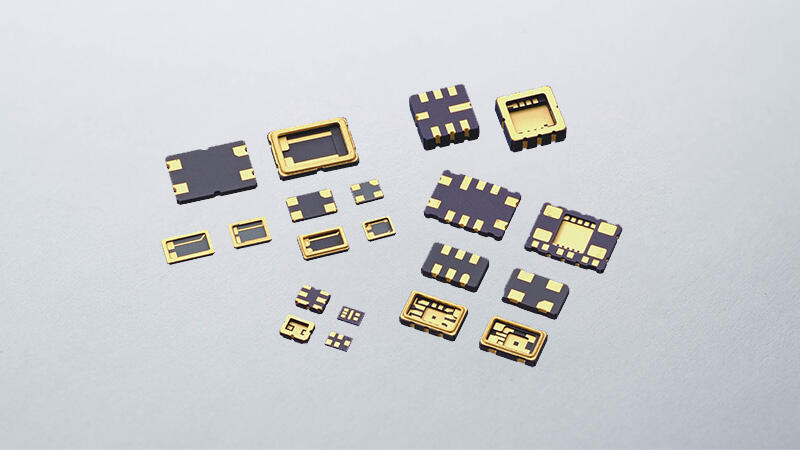
Surface Mount
Leaded
Standard Parts List
Standard Parts List

Standard Parts List
Standard Parts List
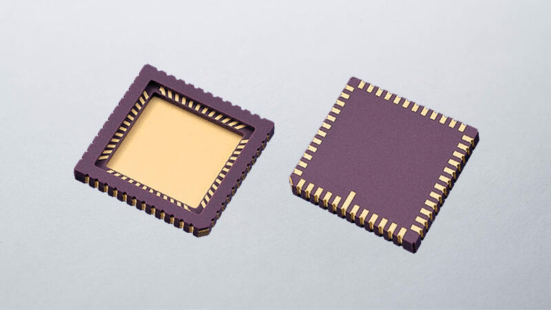
Leadless
Standard Parts List
Standard Parts List
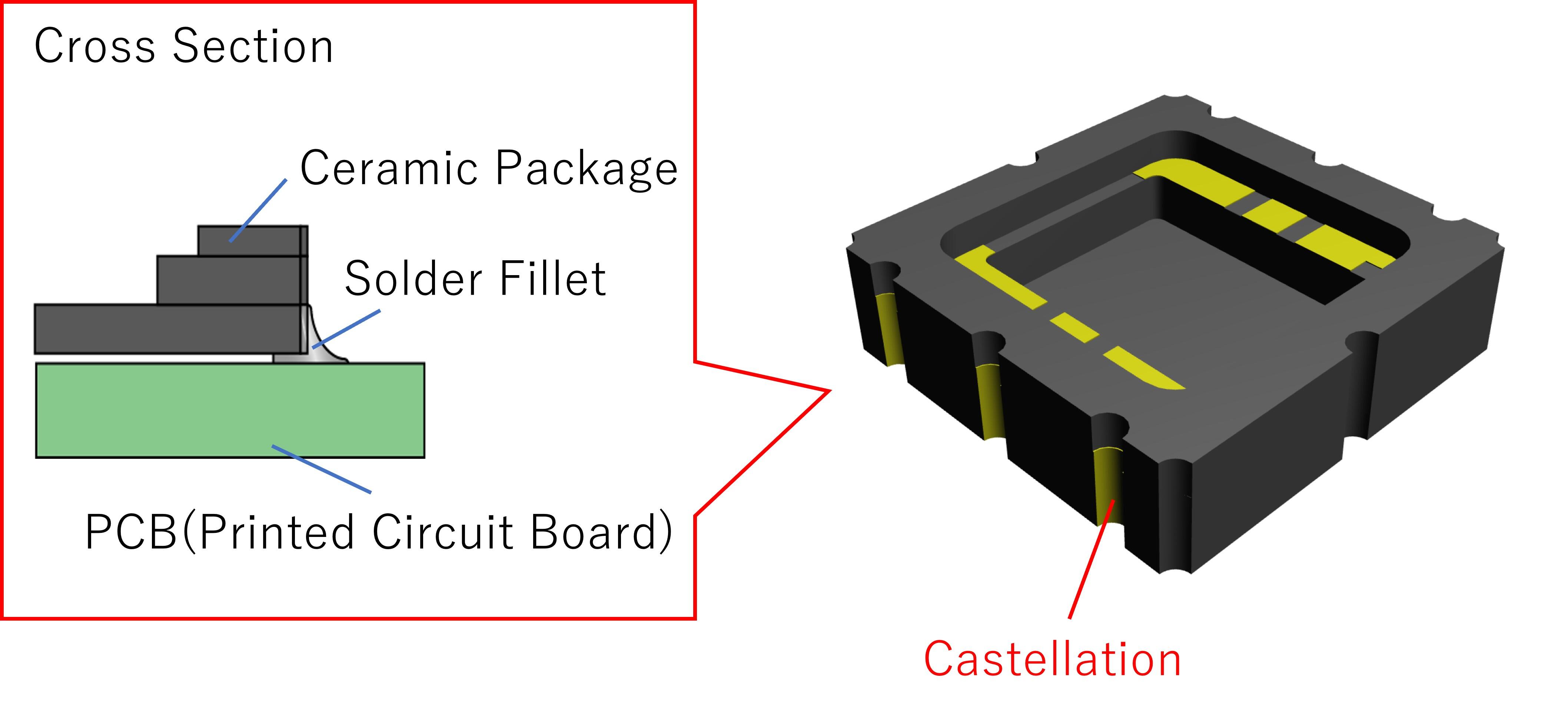
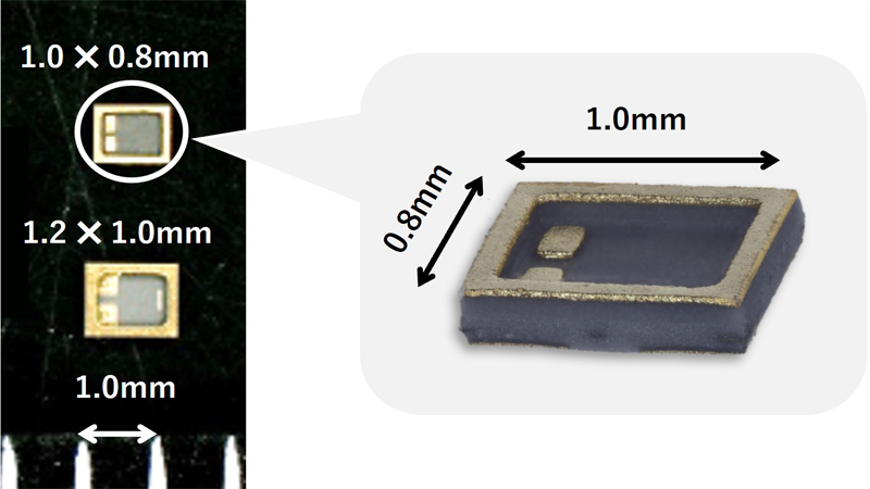
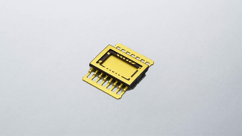
About Castellations on Surface-Mount Device Packages
The sides of a surface-mount package can be designed for electrical connection using metallized castellations.
Castellations enable the formation of solder fillets during board-level assembly, which ensure stronger solder joints and simplify visual inspections.