


Fine Ceramics, sometimes referred to as "advanced ceramics," are engineered materials that support the development of cutting-edge technology.
The Kyocera Museum of Fine Ceramics
Key Player in Semiconductor Production
Characteristics/technologies/applications of Fine Ceramics and the future
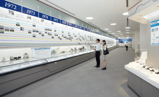
The Kyocera Museum of Fine Ceramics opened in 1998 on the second floor of the Global Headquarters building. It includes exhibits introducing the history of fine ceramics technology and product development. We recently completed a full-scale renewal of the Museum with further enhancements to make the fine ceramics story easier to understand – not only for students and researchers, but also for the general public.
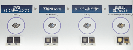
Kyocera' s Technology and Product Evolution
Basic Understanding of Fine Ceramics
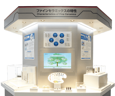
Characteristics of Fine Ceramics
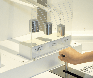
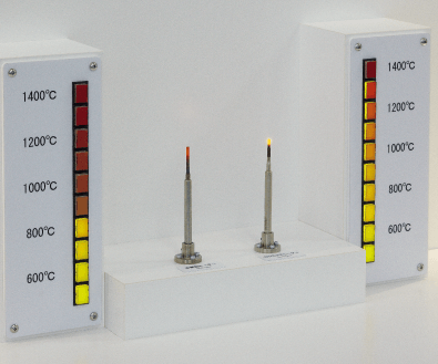
This area showcases the superior characteristics of fine ceramics including their high degree of hardness, rigidity, piezoelectricity and heat resistance. Video displays and hands-on exhibits let visitors gain a more thorough understanding of fine ceramics.
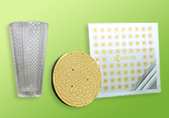
History of Ceramic Packages in the Semiconductor Industry
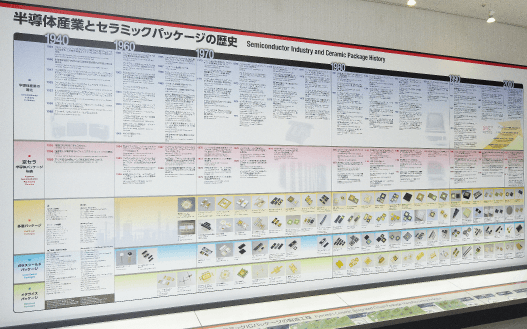
Semiconductors are essential to our highly advanced information society. Here visitors can look back on the history of the semiconductor industry that began in Silicon Valley in the U.S. and see how Kyocera's ceramic packages have been contributing to the industry since its early days.
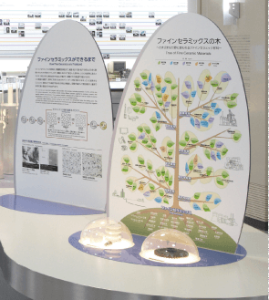
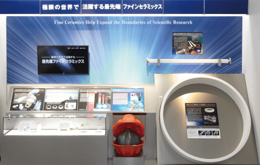
Fine Ceramics Help Expand the Boundaries of Scientific Research
6 Takeda Tobadono-cho, Fushmi-ku, Kyoto, Japan 612-8501
Kyocera Headquarters Building Tel: 81-75-604-3500 (Japan)
People who read this page also read.

What are Fine Ceramics?
What are Fine Ceramics?
Term Coined by the Founder of Kyocera
Term Coined by the Founder of Kyocera
Introduction to Fine Ceramics
Ceramics vs. Fine Ceramics
Ceramics vs. Fine Ceramics
Big Differences in Raw Materials and Production Processing
Big Differences in Raw Materials and Production Processing
Introduction to Fine Ceramics
History of Fine Ceramics
History of Fine Ceramics
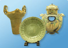
Rooted in Jomon Ware Used Over 10,000 Years Ago
Rooted in Jomon Ware Used Over 10,000 Years Ago
Introduction to Fine Ceramics
If you want to use ceramics in business, click here.
Kyocera's Fine Ceramics products (All websites below open in a separate window.)
Product Category
 Semiconductor / LCD Processing Equipment
 Life / Culture / Industrial Machines
 Wireless Communications
 Computer Peripherals
 Environmental Preservation / Renewable Energy
 Medical Equipment / Devices
 Single-Crystal Sapphire Products
 Metallized / Vacuum Components
 Electronics Industry
 Heaters
 Piezoelectric Ceramics
Search by Material
 Alumina
 Silicon Nitride
 Silicon Carbide
 Sapphire
 Zirconia
 Cordierite
 Yttria
 Aluminum Nitride
 Cermet
 Mullite
 Steatite
 Forsterite
Search by Property/Characteristic


- Thermal Properties
- Coefficient of Thermal Expansion
- Thermal Conductivity
- Heat Shock Resistance

- Electrical Properties
- Insulation / Semiconductivity

- Chemical Properties
- Chemical Resistance
The Fine Ceramics World website is managed by Kyocera Corporation