Challenge: Reduce bonding defects due to Ni diffusion / Improve solderability during board-level assembly
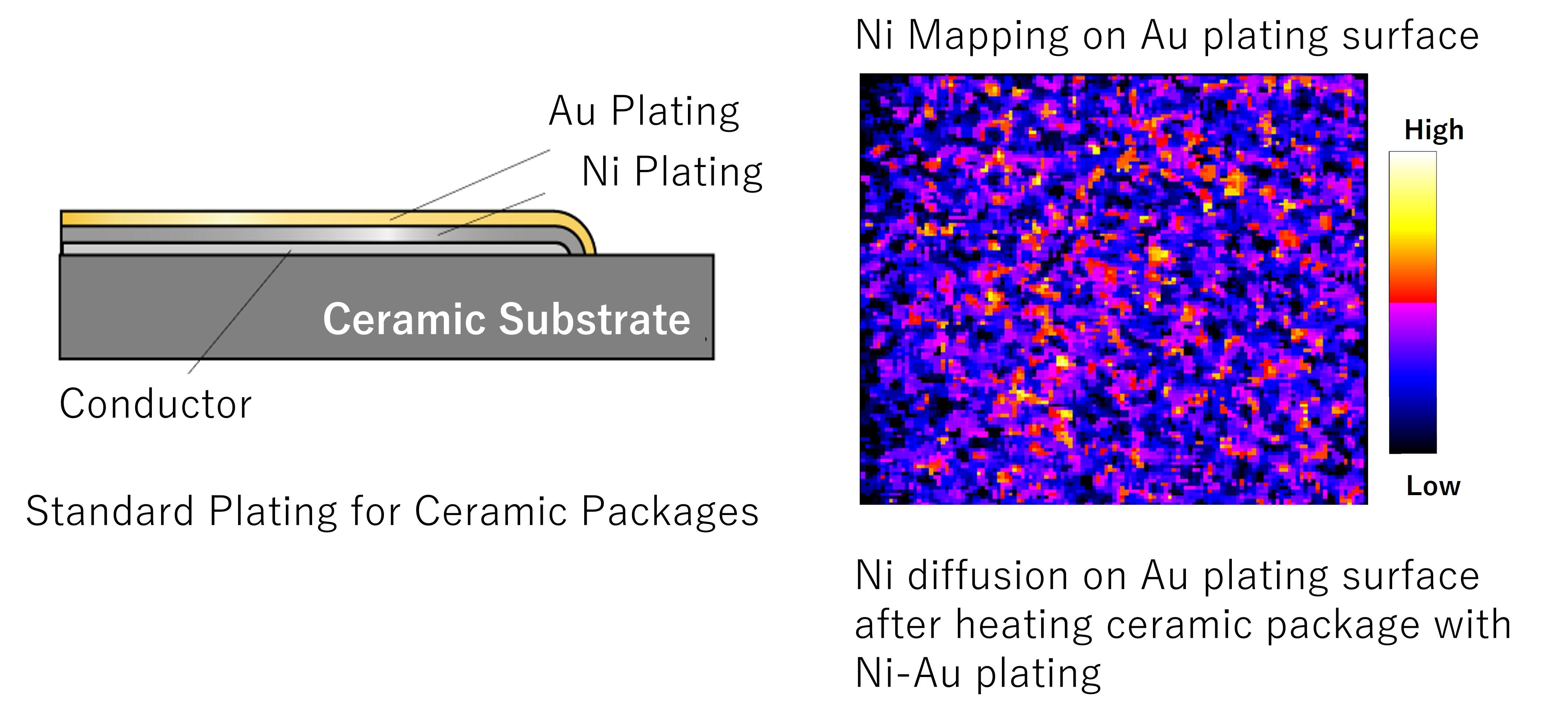
Ni-Au plating is a standard process in manufacturing ceramic packages. However, if the substrate is heated to high temperatures for a prolonged period during chip-level assembly, Ni may diffuse through the Au plating surface, causing Au wire-bonding failures. In addition, applying thicker Au plating to prevent Ni diffusion may cause other reliability issues during the next board-level assembly process.
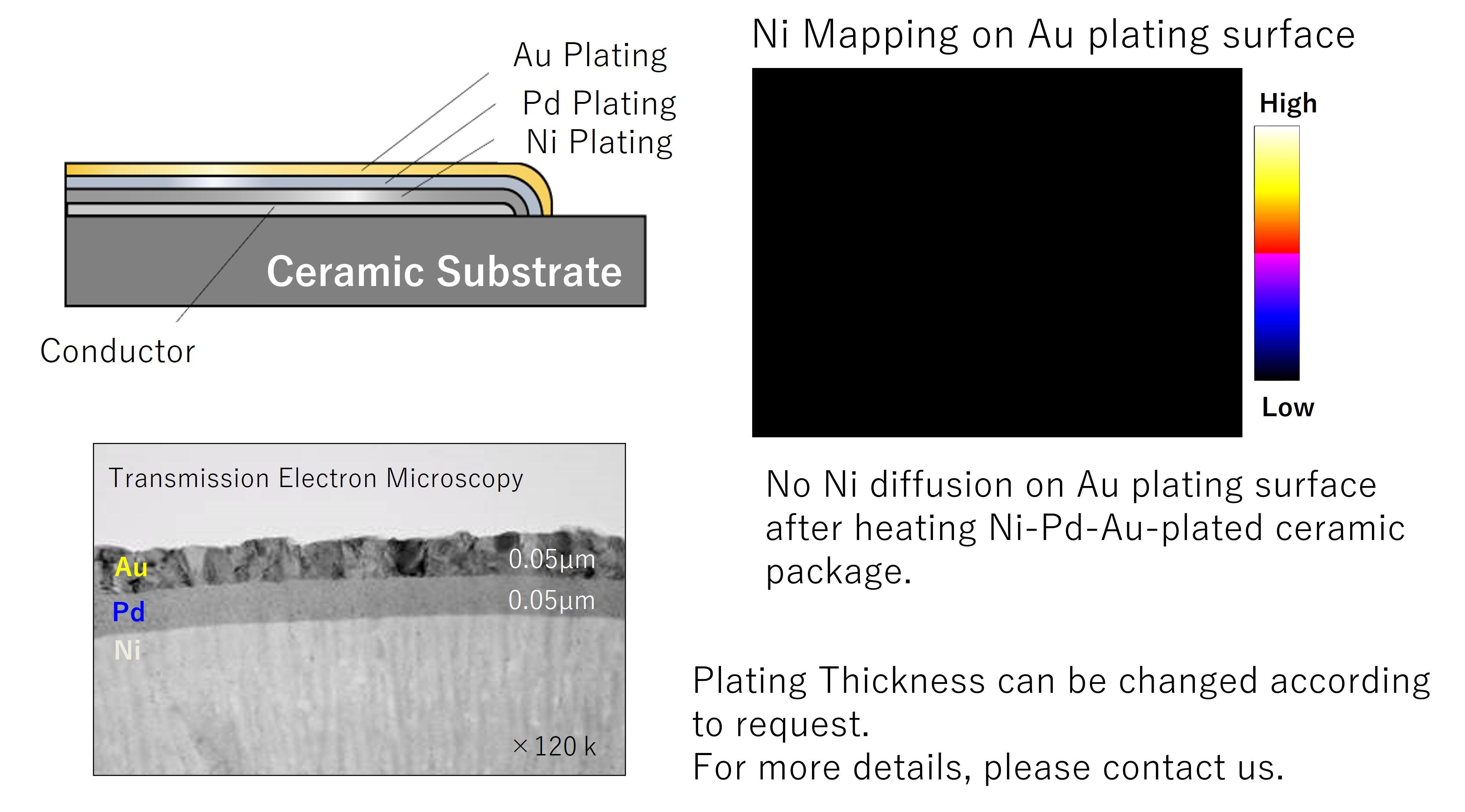
While optimizing Au plating thickness can suppress Ni diffusion, Kyocera also offers a Pd plating layer as an additional barrier to effectively prevent Ni diffusion. Further, by adding a Pd layer, the Au plating can be thinned, which can improve solderability during the next board-level assembly process.
Preventing Ni-Diffusion through Ni-Pd-Au Plating
Plating