Kyocera’s Ceramic Packaging Solutions for
Low Inductance, Heat Dissipation,
and Miniaturization
Inductance, heat treatment, and size are issues for implementing long-range detection functionality in LiDAR.
Kyocera develops Ceramic Package solutions with 1.Low Inductance, 2.High Heat Dissipation, and 3.Compact Size for Pulse and FMCW LiDAR devices.
INTRODUCTION
Industry Efforts to Realizing
Fully Autonomous Driving
Demand around the world is increasing for automated driving to reduce traffic accidents and alleviate traffic congestion.
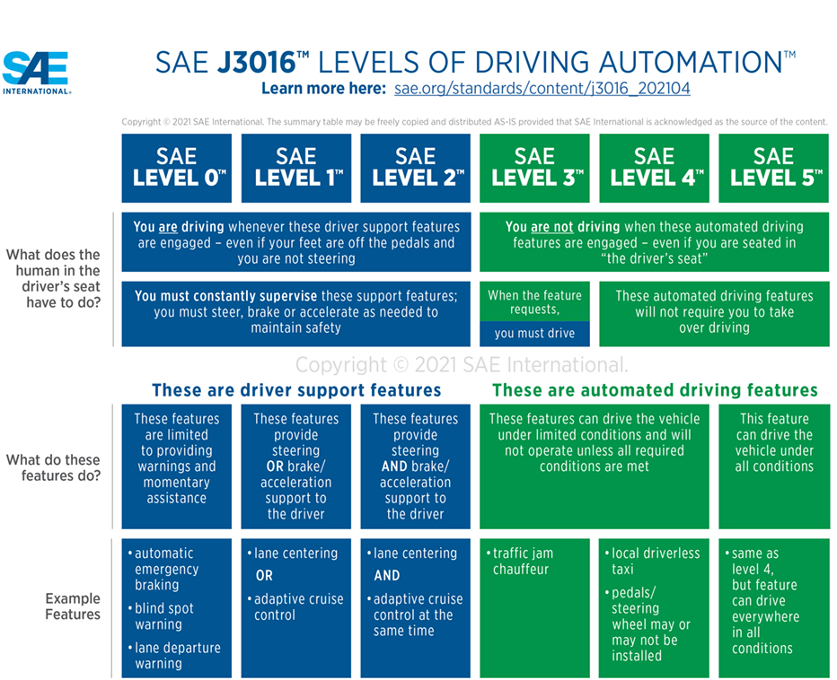
The Society of Automotive Engineers (SAE) classifies autonomous driving into six levels from level 0 to level 5.
At level 5, all driving operations are automated without any restrictions.
Improvement of LiDAR technology is needed to advance system development.
Accelerating The Evolution of Laser Devices
To realize higher-level automotive LiDAR technologies, laser devices are expected to improve further.
Laser devices will play an indispensable role in detecting objects and are a critical element in further developing autonomous driving technology.
Kyocera develops ceramic package solutions for the long-range detection, high-resolution, and miniaturization required for laser devices.
01Long-Range Detection
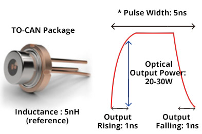
Low inductance is an issue for narrowing pulse width.
In order to detect distant objects more clearly, it is necessary to increase the output power of the laser device.
However, due to eye-safe restrictions, the pulse width must be cut in half to double the irradiation distance.
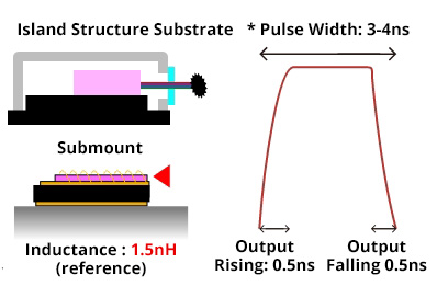
Therefore to narrow the pulse width, low inductance must be achieved.
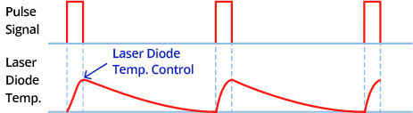
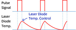
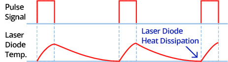
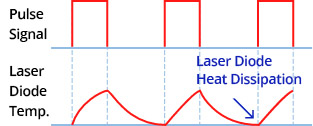
Controlling the temperature rise of laser diodes is an issue to increase output power.
Although long-range detection is possible by increasing the laser output power, the temperature rise of the laser diode can lead to failure.
Ceramic Package Specialized for
Low Inductance and Heat Dissipation
Low Inductance
Factors that increase inductance include wire length, lead length, and electric routing inside the package.
However, low inductance can be achieved by multilayer ceramic packages with a flip-chip design, surface mount design, and multi-VIA design.
-
Conventional TO-CAN Package
-
Ceramic Package Technology
-
Heat Dissipation
-
By narrowing the pulse width, the temperature rise of the laser diode is suppressed.
-
If the pulse width is not narrowed, it is also possible to suppress the laser diode’s temperature rise, improving the heat dissipation of the package.
・Structural Design Solution
Ceramic package designed to widen the heat path and structurally suppress the temperature rise.
・Material Solution
High thermal conductivity ceramic improves heat dissipation.
-
-
Solution
- Narrow pulse width (laser diode calorific value suppression)
- Improve heat dissipation of pulsed laser diode
02High Resolution with Compact Design
-
Multi-channel designs can be difficult for module miniaturization.
Multi-channel technology is required for high-resolution detection and can’t be supported with single channel devices. Multilayer ceramic packaging provides this flexibility.
In addition, the mounting density of the laser diode can increase the temperature rise and may result in device malfunction. -
Single Channel
Package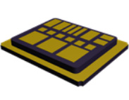
Multi-Channel
Package
Compact Design through
Unique Ceramic Shape
Leveraging the customizable shape formation of multilayer ceramic substrates, Laser diodes / Driver IC / Monitor PD / passives are mounted in 2D or 3D and are electrically connected by circuit pattern in ceramic.
The result is multilayer ceramic with shortened wiring length (narrow pulse).
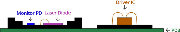


- Chip size
(Estimation) -
- Monitor PD:1×1mm
- Laser Diode:5×4mm
- Driver IC:3×6mm
1. and 2. 25% Surface Area Reduction and Lower Inductance
3. 40% Surface Area Reduction and Lower Inductance
Taking Autonomous Driving Technology to the Next Level!
The automotive industry continues to innovate in various areas toward the early commercialization of level 5 fully automated driving.
Kyocera’s ceramic packaging solutions are critical for this technology advancement to support automotive LiDAR.
Kyocera continues to strive to develop and improve our technology solutions and to supply ceramic packages that enhance the safety and security of autonomous driving.
Kyocera offers the best package solution for the issues you are facing in product development.