Case Studies
Case Study(1960s–1970s)
World Dominance
in Ceramic Multilayer Packages
Taking a forward-looking view of the company’s capabilities
unified company-wide technological development
Looking to the future of semiconductors and tackling goals beyond current capabilities
In the late 1960s, in the early years of the semiconductor industry, Kyocera undertook a major challenge that would start the company’s journey to becoming the world's leading ceramics manufacturer. The project involved a large order from a US manufacturer for the development and mass production of ceramic multilayer packages. Such packages are ceramic "containers" that protect extremely delicate integrated circuits from corrosion and dust, and they were indispensable for the further development of semiconductors. But developing and mass-producing the packages presented an unprecedented technological challenge and required massive capital investment. The driving force for overcoming those obstacles was Kyocera’s determination to strengthen its capabilities, so that goals seemingly impossible at the time could be achieved at some point in the future.

When facing a demand for new technology, first accept the challenge by saying, "It can be done"
- #New Challenges
In 1969, Kyocera received an order from Fairchild Electronics Corporation in the United States to produce 50 units of a prototype high-density ceramic multilayer package for large-scale integration devices. Representing a groundbreaking concept for its time, the package comprised two ceramic substrates stacked and connected by 92 extremely small through-hole vias. Kyocera promised to produce the prototypes in three months. Rather than thinking about whether that was possible based on existing capabilities, Kyocera deliberately set a goal beyond available capabilities to be achieved at a specific point in the future. This spirit of challenge was the key to propelling the development project forward. Despite lacking the necessary equipment, Kyocera staff worked tirelessly, literally forgetting to eat and sleep, and delivered the prototypes within the promised deadline. Although the prototype was ultimately not adopted due to design changes by the client, the technological breakthroughs achieved by Kyocera during the development process — such as tape molding technology, ceramic lamination technology, and co-firing technology — became the foundation for establishing Kyocera’s solid reputation among the world’s leading semiconductor manufacturers.
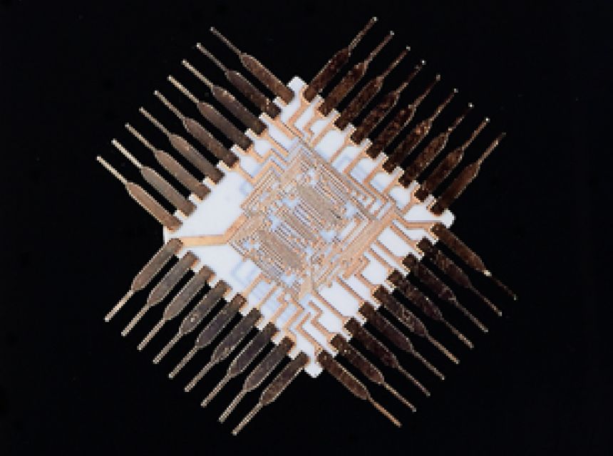
High-density package
Mass production order demands major investment and bold action for future growth
- #Making the Right Decisions
Not long after the success of the prototype project, Kyocera received a huge order in August 1969 from American Microsystems in the United States for one million ceramic multilayer packages for integrated circuits used in calculators. Due to the significant investment required for mass production, the project was difficult for the leading US ceramics manufacturers to handle. But Kazuo Inamori, then company president, was convinced of the future potential of semiconductors and immediately decided to accept the order. Despite Inamori’s standard policy of using only existing equipment and his cautious investment approach, he decided to commit a massive investment of 700 million yen over 3 years, a sum equivalent to 30% to 40% of the company's annual pre-tax profit at the time. His decision was the realization of the Kyocera Philosophy “Be Bold and Meticulous,” as it was based on a vision of the future potential of semiconductors and not on trends of what other companies were doing or on the industry status quo. And it marked a crucial turning point in Kyocera's rise to become the world's leading manufacturer of fine ceramics.
Despite lacking equipment, Kyocera’s ingenuity and perseverance forged a path
- #Dedicated Effort
However, the path to mass production was far from smooth. Because suitable production equipment did not exist in the ceramics industry, the tape molding process began with a trial-and-error approach in which staff would place the tape coming out of the molding machine onto wooden boards and cut it with roller cutters. Even after a year, mass production at the Kagoshima Plant was still not on track, and monthly losses continued to mount. Inamori himself frequently visited the plant, discussing the problems with the production staff and tenaciously searching for ways to improve the process. Thanks to the efforts of the members involved, the yield finally improved by the end of 1970, and in April 1971, a system for producing one million units a month was established.
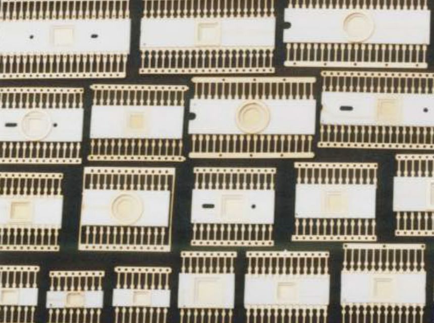
Early ceramic multilayer packages
A technological innovation that produced an “industry staple,” and the spirit of challenge that continues today
- #New Challenges
Successful mass production, combined with the growth in calculator demand, greatly boosted Kyocera's business performance even during the recession caused by the “Nixon Shock” (US suspension of the gold standard). Kyocera subsequently grew to capture approximately 80% of the global semiconductor package market in this field, and received prestigious awards such as the Okochi Memorial Grand Prize for Production. As Inamori said, “Anyone can judge what is possible or impossible based on existing capabilities, but nothing new can be achieved that way.” Even when customer demands exceeded the company's technological capabilities, Kyocera’s staff poured their hearts and souls into development. This spirit of challenge and creativity, and the forward-looking view of future potential that the company cultivated through the development of ceramic multilayer packages, became the driving force behind the later growth of the Kyocera Group.
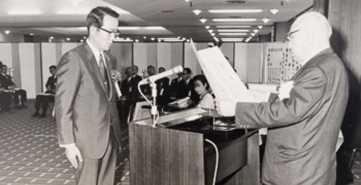
Inamori receiving the Okochi Memorial Grand Prize for Production in 1972


