Kyocera's proprietary technologies(Technologies owned by Kyocera)
Introducing the technology Kyocera has cultivated in thermal printheads.
Proprietary Technology Cultivated in Thermal Printheads
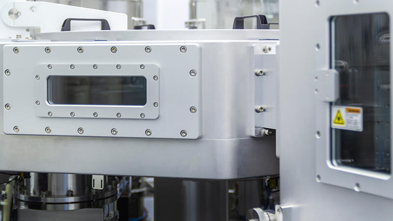
Thin-Film Deposition Technology
With the film deposition technology cultivated in thermal printheads, various materials from conductive materials to insulating materials can be deposited with film thicknesses ranging from several 10 nm to several μm. Various deposition methods are employed to maximize high quality and required performance. Kyocera also possess a production environment capable of mass production.
Use cases: Deposition of resistive film, electrode film, and protective film
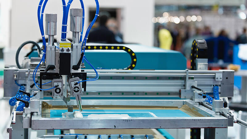
Screenprinting Technology
Screen printing technology developed for thermal printheads can be used to form conductive to insulating materials with a film thickness of several tens of microns. We select materials that provide the high quality and performance required. Kyocera also possess a production environment capable of mass production.
Use cases: Pattern and protective layer printing formation
Photolithography Technology
Photolithography technology developed for thermal printheads can be used to form thin films of conductive materials, such as resistive films and electrode films in a line-and-space formation of a few microns.The high precision of the wiring formation ensures high quality and stable performance. Kyocera also possess a production environment capable of mass production.
Use cases: Heater and pattern formation
Plating Formation Technology
Plating can be formed on metal electrodes with a film thickness of several microns using plating formation technology developed for thermal printheads. It is possible to form even complex pattern shapes and form uniform plating thickness. Furthermore, excellent solderability ensures high reliability of the finished product. Kyocera also possess a production environment capable of mass production.
Use cases: Plating process for bonding driver ICs and electrical components
Assembling Technology
Mounting technology developed for thermal printheads enables mounting of high-density flip chips with an accuracy of several tens of microns. Kyocera also possesses solder bump formation technology for flip chip mounting of driver ICs.We also possess assembly technologies such as flexible printed circuit board (FPC) and ceramic substrate bonding technology, and have production environments in Japan and overseas that enable mass production.
Use cases: Mounting and joining of driver ICs and electrical components; formation of solder bumps for flip chips