This news release is intended for media purposes, and is current of the date of publication. Information is subject to change without notice.
KYOCERA Breaks Ground on New Manufacturing Plant for Ceramic Microelectronic Packages in Kagoshima, Japan
New facility to increase capacity by 25%, support IoT growth with ceramic packages for electronic and semiconductor components including SMD and CMOS devices
June 20, 2018
Kyocera Corporation (President: Hideo Tanimoto) held a groundbreaking ceremony on June 20, 2018 for a new plant at its Kagoshima Sendai manufacturing complex in Japan. The company aims to increase production of ceramic microelectronic packages to accommodate robust demand and to expand related businesses in the future.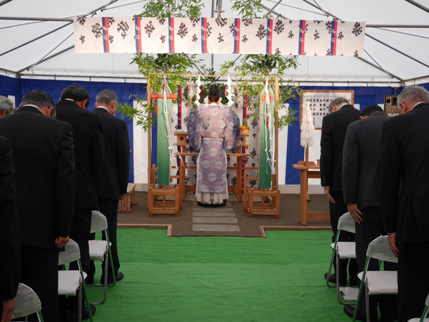
Groundbreaking Ceremony
The new facility, which Kyocera plans to open in August 2019, will bring a 25 percent increase in the company's total production capacity for ceramic packages used to house SMD*1 electronic devices and CMOS*2 image sensors, and will allow the company to expand production for other items depending on future needs. Kyocera entered into a site location agreement with the governor of Kagoshima Prefecture and the mayor of Satsumasendai earlier this year.
The electronics industry is now experiencing new growth fueled by big data, artificial intelligence, and the Internet of Things (IoT). The development of advanced driver-assist systems (ADAS) and technology that supports minimally invasive medical treatments will drive future growth as well. The new Sendai facility will significantly increase Kyocera's production capacity for two key enablers of these applications — SMD ceramic packages and packages to house CMOS image sensors — as well as ceramic packages for automotive and medical devices.
Details of the New Plant
| Name | Kyocera Corporation Kagoshima Sendai Plant (the 22nd facility on the premises) |
| Location | Kyocera's Kagoshima Sendai Manufacturing Campus, 1810 Taki-cho Satsumasendai, Kagoshima 895-0292 Japan |
| Total investment | Approximately 5.9 billion yen (approx. USD 53.6 million) |
| Building area | 8,235m2 steel construction with 6 stories |
| Total floor space | 42,283m2 |
| Construction plan | Begin construction: June 2018; start manufacturing: August 2019 |
| Main products | SMD ceramic packages, ceramic packages for CMOS image sensors |
| First-year production plan | Approximately 3.8 billion yen (from August 2019 through March 2020) |
*2 CMOS: Complementary metal oxide semiconductor