Notable Moments
Major decisions in the semiconductor package business (1970)
In 1969, Fairchild Semiconductor in the United States asked Kyocera to prototype 50 high-density multilayer ceramic packages for use in Large Scale Integration (LSI) devices. These packages were a revolutionary new concept, and Kyocera took on the prototyping with the promise that they could be produced in three months.
Integrated circuits are very delicate, and require protection to shield them from corrosion and dust. The ceramic "container" providing protection is the package.
When the integrated circuit was invented in the U.S. in 1959, the U.S. had the world's largest ceramic manufacturers, far bigger than Kyocera. Silicon Valley semiconductor manufacturers such as Intel approached those large ceramic manufacturers, but they hesitated to make deals that would involve large capital expenditures because they were unsure about the future of semiconductors.
By contrast, based on his experience in the production of transistor components and substrates for hybrid integrated circuits, Inamori was convinced that integrated circuits would definitely grow into a major industry. In response to an inquiry from Fairchild Semiconductor for package development, Inamori decided to build a dedicated production line in Japan. Kyocera's sales at that time were 7 billion yen. Inamori committed 700 million yen of capital investment - or 50% of annual capex - for two years running to establish facilities and production methods, by doing so embracing the challenge of the semiconductor package business. It was this decision that launched Kyocera - a clear newcomer as a ceramic manufacturer - into the world's elite.
As a manager, Inamori had always been very cautious about capital investment. He used existing facilities to their full potential and purchased new facilities only after production delays started happening. However, when Inamori entered the semiconductor package market, he made a bold investment by sparing no expense on the necessary facilities.
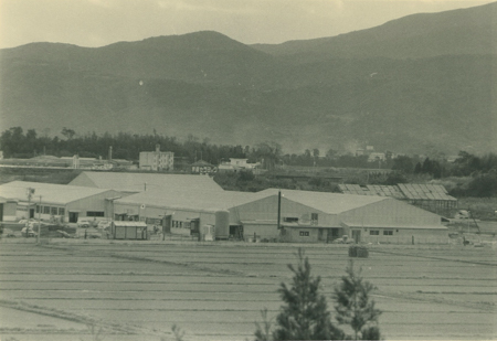
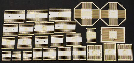
Photos
1: Kagoshima Sendai Plant, where large-scale investment was made for semiconductor packages
2: The early multilayer ceramic packages that powered the company's success
