Technology
Ceramic Multilayer Package
In 1969, Kyocera received a prototype request from Fairchild Semiconductor in the United States to develop a ceramic multilayer package for LSI devices, known as the High-Density Package (HDP). This design, stacking two ceramic substrates and connecting them with 92 via holes, was a remarkably advanced concept at the time. Since Kyocera had already been researching core technologies in this area, Inamori confidently promised, "We can deliver it in three months," and immediately launched development efforts.
Behing this seemingly bold commitment was Inamori's prior experience visiting Texas Instruments (TI), where he had been asked to prototype a new package to protect integrated circuits. Recognizing that new ceramic technologies were emerging in the U.S. and intuitively sensing their potential to become a major industry, Inamori returned to Japan and began developing tape-casting and lamination methods. His foresight and preparation enabled Kyocera to meet the challenging deadline.

【High-Density Package】
The development of the world's first ceramic multilayer package was far from easy. The team faced numerous technical challenges, including ensuring tape strength and dimensional stability, processing via holes, printing fine circuits, and achieving precise lamination, all while working with limited equipment. Inamori and his engineers worked tirelessly, even procuring specialized machinery from overseas. Their relentless efforts finally paid off when they completed the prototypes and delivered 20 units to Fairchild as promised, earning high praise.
Although the HDP was ultimately not adopted due to design changes, the development process resulted in significant technological advances in tape casting, lamination, and co-firing. These breakthroughs later became the foundation for large-scale orders from companies such as American Microsystems, Inc. (AMI) and Intel.
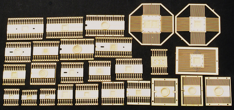
【Ceramic Multilayer Package from the early production period】
In August of the same year, Kyocera received a major order from AMI for one million IC packages for calculators. Although Inamori was generally cautious about capital investment, he was convinced of the semiconductor industry's future potential. He made a bold decision to invest 30-40% of Kyocera's pre-tax profits in new facilities and production lines, a move that many U.S. manufacturers hesitated to make amid uncertainty. This decision marked a turning point, paving the way for Kyocera's growth into a global leader in fine ceramics.
Mass production, however, was not without difficulties. The Kagoshima plant (currently Kagoshima Sendai Plant) struggled with equipment shortages and low yield rates, resulting in continued losses. Inamori frequently visited the site, working closely with employees and executives to drive improvements. Many of those who supported him during this period would later become key members of Kyocera's leadership team. By the end of 1970, yield rates had improved significantly, and by April 1971, Kyocera achieved a monthly production capacity of one million units. Despite an economic downturn, strong demand for calculators fueled the company's growth. Kazuo Inamori's decisive leadership, foresight, and hands-on approach transformed Kyocera into one of the world's leading semiconductor package manufacturers. This experience became a driving force behind the company's continued growth and its evolution into a global enterprise.
